CARA CETAK PCB MANUAL Paling mudah anti gagal
Summary
TLDRThis tutorial guides viewers through the process of creating a custom PCB (printed circuit board) from scratch. The video covers each step, from selecting materials like the FR4 PCB board and preparing layout prints, to applying the design and etching the circuit using ferric chloride. It emphasizes the importance of patience, precision, and care in achieving professional-quality results, even with manual methods. The host shares tips on cleaning, drilling, and finalizing the board, offering a clear and accessible guide for DIY electronics enthusiasts. The tutorial promises a simple yet effective way to create durable, high-quality PCBs at home.
Takeaways
- 😀 The process of making a DIY PCB involves several key steps: printing, transferring the layout, etching, and drilling the board.
- 😀 FR4 PCB material is recommended for durability, and it's essential to use a thick board for better results in etching.
- 😀 Ensure that the printed PCB layout is photocopied twice to make the toner thicker, which helps prevent issues like corrosion in the traces.
- 😀 Autan mosquito repellent, mixed with water, is used for transferring the printed layout onto the PCB using a mika plastic sheet for pressing.
- 😀 Sanding the PCB with fine sandpaper helps smooth the surface before transferring the layout and ensures better adhesion of the toner.
- 😀 The etching process is done using ferric chloride mixed with warm water. The board must be immersed in this solution until the copper traces become visible.
- 😀 After etching, rinse the PCB to stop the chemical reaction and remove any leftover etchant, ensuring no residue is left on the board.
- 😀 Drilling holes in the PCB for components should be done carefully using a manual drill. Ensure accuracy to fit the components perfectly.
- 😀 Always clean the PCB after every stage—before printing, after etching, and before drilling—to avoid any contamination or defects.
- 😀 Patience and precision are crucial when transferring the layout and during the etching process to achieve clear, accurate PCB traces.
Q & A
What is the purpose of the video?
-The purpose of the video is to provide a step-by-step tutorial on how to manually create a printed circuit board (PCB), including the materials, techniques, and tools required for the process.
Why did the presenter decide to make this tutorial?
-The presenter made the tutorial in response to viewer requests for help on how to print and create their own PCBs after receiving requests for layouts and designs, particularly for a speaker protector PCB.
What materials are needed for making the PCB?
-The materials required include a FR4 PCB (preferably thick), printed layout (photocopied), Autan (a mosquito repellent) mixed with water, a plastic sheet, and tools such as fine sandpaper, a cutter, and a drill.
Why does the presenter use two layers of photocopied paper for the toner transfer?
-The presenter uses two layers of photocopied paper to ensure that the toner is applied thickly, preventing the copper tracks from corroding or becoming weak, ensuring a cleaner and more durable result.
What is the role of Autan in the PCB creation process?
-Autan, mixed with water, is used to help transfer the toner from the photocopied design onto the PCB. It is spread on a plastic sheet that is pressed onto the PCB to ensure a clean and sharp transfer of the circuit layout.
What should be considered when applying pressure during the toner transfer process?
-The presenter advises to apply moderate and even pressure when pressing the plastic sheet onto the PCB. Too much pressure can distort the design, while too little might result in incomplete transfers.
What happens if the toner transfer is not done properly?
-If the toner transfer is not done properly, the PCB may have incomplete or distorted copper traces, which can lead to malfunctioning circuits. The presenter emphasizes the importance of careful, patient work to achieve a perfect transfer.
What is the purpose of the ferric chloride (perclorid) solution in the process?
-Ferric chloride is used to etch the PCB, removing excess copper and leaving behind only the desired circuit traces. It is a crucial step in the creation of the PCB design.
What steps are involved in the final PCB cleanup?
-After etching, the PCB is cleaned to remove any remaining ferric chloride solution, ensuring no corrosion. The PCB is also dried, and any excess paper or toner is carefully removed before final drilling and component mounting.
What advice does the presenter give for ensuring a successful PCB creation?
-The presenter advises patience, precision, and careful handling throughout the process. Reapplying the toner to make it thicker and performing the steps slowly and methodically can result in a PCB of similar quality to those produced by professional manufacturers.
Outlines

このセクションは有料ユーザー限定です。 アクセスするには、アップグレードをお願いします。
今すぐアップグレードMindmap

このセクションは有料ユーザー限定です。 アクセスするには、アップグレードをお願いします。
今すぐアップグレードKeywords
このセクションは有料ユーザー限定です。 アクセスするには、アップグレードをお願いします。
今すぐアップグレードHighlights

このセクションは有料ユーザー限定です。 アクセスするには、アップグレードをお願いします。
今すぐアップグレードTranscripts

このセクションは有料ユーザー限定です。 アクセスするには、アップグレードをお願いします。
今すぐアップグレード関連動画をさらに表示
How to Make an Automatic Emergency Light || Power Failure Backup Light
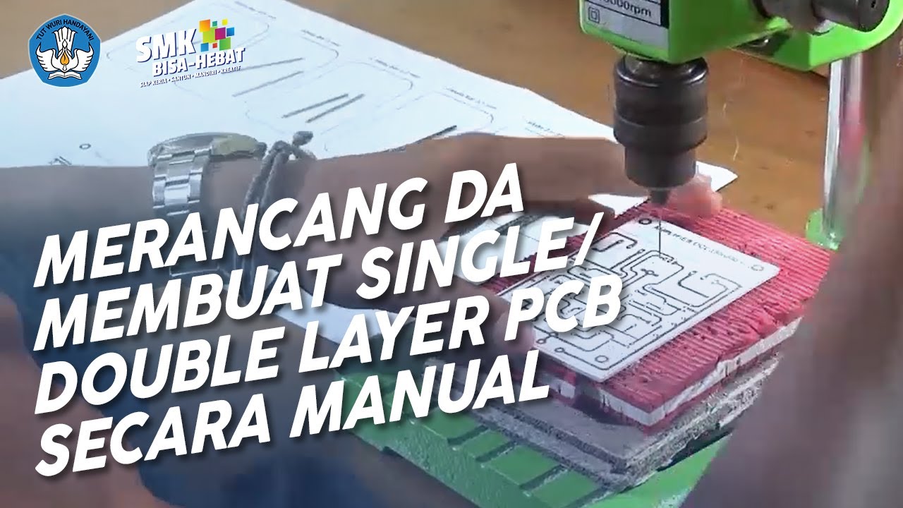
Merancang dan Membuat Single/ Double Layer PCB secara Manual dengan Metode Eksposure

Kicad Beginner Tutorial- A Traffic Light for Arduino ( RE-UPLOADED, Twice )
pH meter Arduino, pH Meter Calibration, DIYMORE pH Sensor, pH Sensor Arduino Code, pH of liquids

Scratch - Membuat Game Flappy Bird

STM32F4 Programming in C 1- LED Blinky coding in Keil using STM32CubeMx
5.0 / 5 (0 votes)
