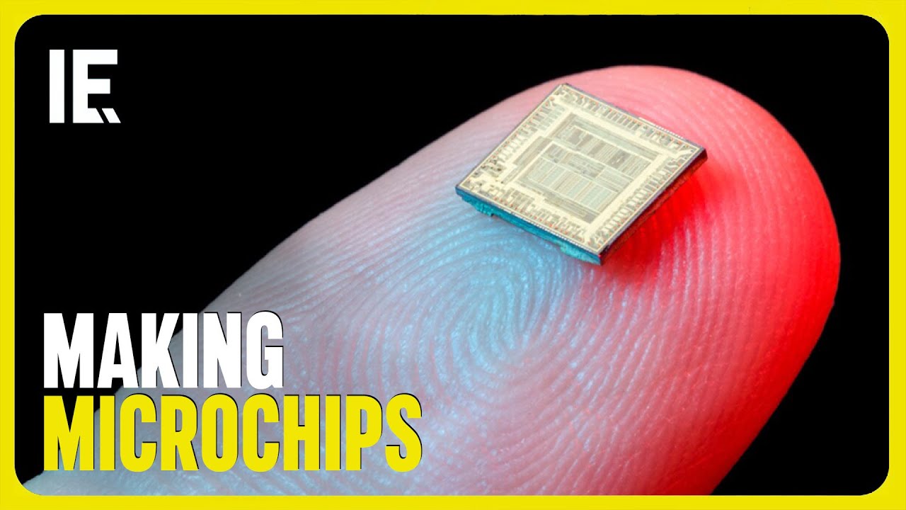
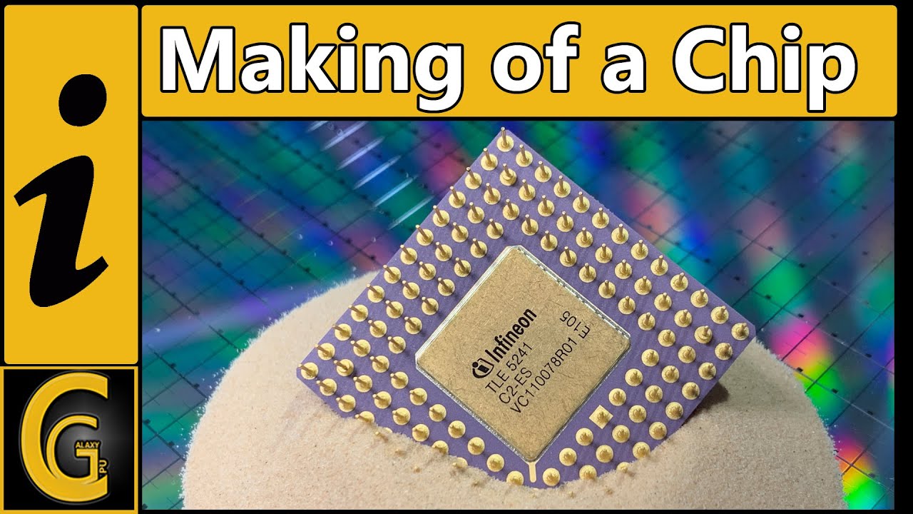
Chip Manufacturing - How are Microchips made? | Infineon

Infineon Technologies
17 Jul 201913:32

Summary

TLDRThis script outlines the intricate process of semiconductor manufacturing, starting from raw sand to finished chips. It details the transformation of silicon dioxide into pure silicon ingots, followed by slicing into wafers. The semiconductor nature of silicon is harnessed through doping to create P and N-type layers, essential for transistor construction. The script further explains the fabrication process involving photolithography, oxidation, etching, and metallization, all conducted in a cleanroom to ensure precision. The final steps include assembly and packaging, highlighting the importance of quality control for producing reliable semiconductor devices.

Takeaways

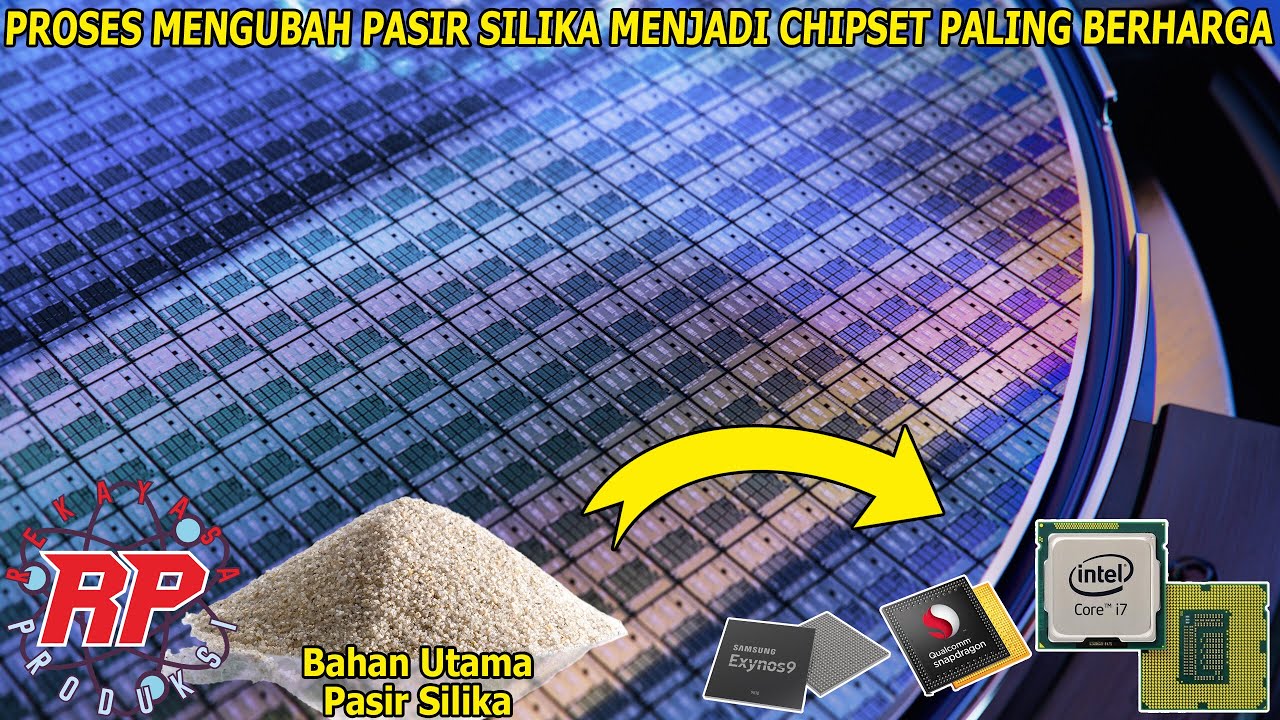
  • 🏗️ Sand, primarily composed of silicon dioxide, is the starting material for semiconductor chips.
  • 🔥 A high-temperature process involving carbon is used to remove oxygen from silica sand, creating pure silicon.
  • 🔬 Silicon is a semiconductor material that can conduct electricity and act as an insulator.
  • 🔋 Doping with impurities like boron or phosphorus alters silicon's conductivity to create n-type or p-type semiconductors.
  • 🔩 Transistors, built on doped silicon layers, control electric voltages and currents and are crucial for microchips.
  • 🛠️ The chip fabrication process requires a cleanroom environment to prevent contamination.
  • 📏 Photo masks are used to transfer circuit designs onto silicon wafers through a process involving light exposure and etching.
  • 🔍 Scanning electron microscopes are utilized to ensure the quality and precision of the chips at various production stages.
  • 🔗 The final stage of fabrication involves assembling the individual chips into packages with terminals for circuit board mounting.
  • 🌐 Microelectronics are integral to modern life, enabling innovations that improve safety, efficiency, and accessibility of technology.

Q & A

  • What is the primary component of sand used in chip manufacturing?

    -The primary component of sand used in chip manufacturing is silicon dioxide or silica.

  • How is silicon extracted from sand in the chip-making process?

    -Silicon is extracted from sand by combining it with carbon and heating it to an extremely high temperature to remove the oxygen.

  • What is the term for the extremely pure mono crystalline silicon used in chip manufacturing?

    -The extremely pure mono crystalline silicon used in chip manufacturing is called a silicon bull or ingot.

  • What are the most common diameters for silicon wafers?

    -The most common diameters for silicon wafers are 150, 200, and 300 millimeters.

  • Why are large diameter wafers preferred in chip manufacturing?

    -Large diameter wafers are preferred because they offer more space for chips, which can increase production efficiency.

  • What is the role of doping in the silicon wafer process?

    -Doping is the process of adding small quantities of specific atoms to the silicon wafer to make it conductive. Elements from the thirteenth or fifteenth group of the periodic table are used for this purpose.

  • What are the two types of conductive layers created by doping?

    -The two types of conductive layers created by doping are n-type, which is conductive with the addition of phosphorus, and p-type, which is conductive with the addition of boron.

  • What is a transistor and how does it function?

    -A transistor is the smallest control unit in microchips that controls electric voltages and currents. It can be switched between current flow (on) and no flow (off) by applying electrical charges to its terminals.

  • How are the layers for transistors created on a wafer?

    -The layers for transistors are created through a series of steps including oxidation, photoresist application, exposure through photo masks, etching, and doping.

  • What is a cleanroom and why is it necessary for chip fabrication?

    -A cleanroom is a dust-free environment with stable temperature and humidity levels, necessary for chip fabrication to prevent contamination that can ruin the microscopic structures of chips.

  • What happens during the final stage of chip fabrication known as assembly?

    -During the final stage of chip fabrication, individual chips are placed in a package, and terminals are attached to create a finished semiconductor device ready for use.

  • How are power semiconductors different from standard semiconductors?

    -Power semiconductors are designed to switch high electrical currents and voltages, and they often have integrated cooling areas to dissipate the heat generated during operation.

Outlines

00:00

💿 Silicon Wafer Production

This paragraph discusses the process of transforming raw silica sand into silicon wafers, which are the foundational elements for chip production. Silicon, the second most abundant element in the Earth's crust, is refined from sand through a series of complex chemical and physical procedures. The process involves combining sand with carbon and heating it to extreme temperatures to remove oxygen, resulting in pure mono crystalline silicon known as a silicon bull. These silicon bulls are then cut into thin wafers using a special sawing technique. The wafers are essential for subsequent chip production and are made conductive through the addition of impurity atoms like boron or phosphorus, a process known as doping. This doping process allows the silicon to either have an excess of electrons (n-type) or create electron holes (p-type), which are necessary for the semiconductor properties of chips.

05:02

🛠️ Fabrication of Integrated Circuits

The second paragraph delves into the intricate process of creating integrated circuits on silicon wafers. It starts with the design phase, where the chip's functions are defined, its properties are simulated, and its functionality is tested. The design is then transferred to photo masks, which are used to reproduce the microscopic structures of the chip in a dust-free environment known as a cleanroom. The fabrication process includes oxidizing the wafer surface, applying photoresist, exposing it to light through the photo mask, developing the exposed areas, etching off the developed oxide layer, and depositing conductive polysilicon. Further steps involve doping the silicon to alter its conductivity, etching contact holes for interconnections, and depositing metal alloys to create contacts. The process may be repeated multiple times to build up the layers necessary for the integrated circuit. The paragraph also emphasizes the stringent cleanliness and precision required in the production environment to ensure the quality of the chips.

10:06

🔩 Assembly and Quality Control of Semiconductor Devices

The final paragraph outlines the assembly and quality control stages of semiconductor production. After the integrated circuit is complete, individual chips are separated from the wafer, which involves leaving scribe lines and integrating test structures for immediate post-production measurements. The size of the resulting chips can vary significantly. The chips are then assembled into packages with terminals, creating finished semiconductor devices that can be mounted on circuit boards. The paragraph also highlights the use of special packages for power semiconductors designed for high-current applications like electric vehicles and renewable energy systems. The importance of advanced testing technologies and precision equipment in ensuring the quality and functionality of these tiny components is emphasized, as they are critical to the performance and reliability of the devices they are used in.

Mindmap

Keywords

💡Silicon Dioxide

Silicon dioxide, also known as silica, is a compound consisting of one silicon atom and two oxygen atoms. It is the primary component of sand and is crucial in semiconductor manufacturing. In the video, it is mentioned as the starting material for making silicon chips, highlighting its role in the foundational stage of chip production.

💡Mono Crystalline Silicon

Mono crystalline silicon is a type of silicon with a single crystal structure. It is highly valued in the semiconductor industry due to its superior electrical properties. The video describes the creation of a 'silicon bull', which is a pure mono crystalline silicon ingot used as the base for chip manufacturing.

💡Doping

Doping is the process of adding impurities to a semiconductor material to alter its electrical properties. In the video, it is explained that adding boron or phosphorus to silicon changes its conductivity, making it either P-type or N-type conductive, which is essential for creating transistors.

💡Transistors

Transistors are semiconductor devices that amplify or switch electronic signals and electrical power. They are the building blocks of modern electronics. The video emphasizes their importance in microchips, where they control electric voltages and currents.

💡Photoresist

Photoresist is a light-sensitive material used in semiconductor manufacturing to transfer a pattern from a photo mask to a silicon wafer. The video describes how photoresist is applied, exposed, and developed to create the pattern for etching layers in the chip fabrication process.

💡Cleanroom

A cleanroom is a controlled environment designed to reduce contamination, such as dust, airborne particles, and chemical vapors. The video mentions that chips are manufactured in a cleanroom to ensure the microscopic structures of a chip are reproduced flawlessly.

💡Ion Implantation

Ion implantation is a process in which ions are accelerated and embedded into a substrate to modify its physical and chemical properties. In the video, it is used to introduce impurity atoms into silicon to change its conductivity during the doping process.

💡Wafer

A wafer is a thin slice of semiconductor material, such as silicon, on which microelectronic circuits are built. The video explains that wafers are cut from silicon bulls and serve as the base for building chips.

💡Scribing Line

A scribing line is a path left between individual chips on a wafer to prevent damage during the sawing process. The video mentions that chips are not lined up flush with each other due to the scribing line.

💡Semiconductor Device

A semiconductor device is a device that exploits the properties of semiconductors to control the flow of electrical current. The video describes the final stage of fabrication where individual chips are assembled into a package, turning them into finished semiconductor devices.

💡Infineon

Infineon is a semiconductor company that designs and produces a wide range of semiconductor devices. The video concludes by mentioning Infineon, suggesting that the company is involved in the production of the microelectronics discussed throughout the video.

Highlights

Sand, primarily composed of silicon dioxide, is the starting material for chips.

Silicon is the second most abundant element in the Earth's crust.

Complex chemical and physical processes are required to purify silicon for chip production.

Silicon is converted from silica sand by combining it with carbon and heating.

Extremely pure mono crystalline silicon ingots, called bulls, are used in chip production.

Silicon wafers are cut from silicon bulls using a special sawing technique.

Silicon is a semiconductor, capable of conducting electricity and acting as an insulator.

Doping with impurity atoms like boron and phosphorus alters silicon's conductivity.

Transistors, built on doped wafers, are the fundamental control units in microchips.

Transistors control electric voltages and currents, crucial for electronic circuits.

The chip fabrication process begins with layout and design, involving billions of transistors.

Photo masks are used to transfer circuit designs onto silicon wafers.

Cleanrooms with stringent standards are essential for chip fabrication.

Wafers undergo multiple steps including oxidation, photoresist application, and etching.

Doping introduces impurity atoms to change the silicon's conductivity.

Metal alloys are deposited to create contacts and interconnections within the wafer.

Chemical mechanical polishing ensures a smooth finish for the insulation layer.

Final fabrication stages include assembly and packaging of individual chips.

Quality control is maintained through testing at every step of the fabrication process.

Microelectronics play a key role in creating innovative semiconductor solutions for a better future.

Transcripts

play00:00

you

play00:04

all ships start out with a very simple

play00:07

raw material sand sand is primarily made

play00:11

up of silicon dioxide or silica silicon

play00:14

is the second most abundant element in

play00:16

the Earth's crust but is only ever found

play00:18

as a compound with oxygen complex

play00:22

chemical and physical processes are

play00:24

required to ensure that silicon crystals

play00:27

meets the high production standards that

play00:29

apply to chips to convert silica sand to

play00:33

silicon the sand is combined with carbon

play00:36

and heated to an extremely high

play00:38

temperature to remove the oxygen a

play00:40

number of other steps are required to

play00:43

create the finished product namely an

play00:45

extremely pure mono crystalline silicon

play00:47

ingot called a bull with only one

play00:50

impurity atom for every 10 million

play00:51

silicon atoms silicon bulls are

play00:54

fabricated in a range of different

play00:56

diameters the most common sizes are 150

play00:59

200 and 300 millimeters wafers with

play01:03

large diameters offer more space for

play01:05

chips extremely thin wafers are then cut

play01:11

from the silicon Bulls using a special

play01:14

sawing technique these wafers are the

play01:16

basic building blocks for subsequent

play01:18

chip production

play01:22

silicon is a semiconductor this means it

play01:26

can conduct electricity and also act as

play01:28

an insulator it's atomic structure looks

play01:32

like this every silicon atom has four

play01:35

outer electrons there are no free charge

play01:39

carriers as a result the pure mono

play01:42

crystalline silicon is non conductive at

play01:44

room temperature to allow it to become

play01:46

conductive small quantities of specific

play01:49

atoms are added as impurities to the

play01:51

wafer these impurity atoms must have a

play01:53

number of outer electrons that is either

play01:55

one more or one less than that of

play01:57

silicon silicon is in the fourteenth

play02:00

group of the periodic table of elements

play02:02

this means that elements in the

play02:03

thirteenth or fifteenth group have to be

play02:06

used in this process referred to as

play02:08

doping boron and phosphorus atoms are

play02:10

the most suitable elements in these

play02:12

groups they are very close to silicon on

play02:14

the periodic table and therefore have

play02:16

very similar properties phosphorus has

play02:19

five outer electrons when it is inserted

play02:21

into the silicon crystal lattice the

play02:23

fifth phosphorus electron can move

play02:25

freely this means that the silicon

play02:28

phosphorus crystal is n conductive

play02:32

in contrast boron atoms only have three

play02:36

outer electrons when they are introduced

play02:39

into the silicon lattice one silicon

play02:41

electron has nothing to bond to this

play02:44

creates electron holes the holes move

play02:47

through the crystal like positively

play02:49

charged particles making the material P

play02:53

conductive

play02:54

[Music]

play02:56

transistors are built on the P and n

play02:59

conductive layers that exist in a doped

play03:01

wafer transistors are the smallest

play03:04

control units in microchips their job is

play03:08

to control electric voltages and

play03:10

currents and they are by far the most

play03:11

important components of electronic

play03:13

circuits every transistor on a chip

play03:18

contains P and n conductive layers made

play03:21

of silicon crystals they also have an

play03:23

additional layer of silicon oxide which

play03:26

acts as an insulator a layer of

play03:29

electrically conductive polysilicon is

play03:31

applied on top of this every transistor

play03:35

has three terminals the middle one is

play03:38

attached to the gate which is the

play03:40

electrically conductive polysilicon if

play03:44

an electrical charge is applied to only

play03:46

the two outer terminals electricity

play03:49

cannot flow as the transistor is blocked

play03:52

this changes however if an additional

play03:54

charge is applied to the middle terminal

play03:58

electrons from the P layer are then

play04:00

pulled toward the middle terminal and

play04:02

accumulate at the area bordering the

play04:04

silicon crystal and the insulating gate

play04:07

oxide

play04:10

a channel then forms underneath the gate

play04:12

between the islands of n conductive

play04:14

material electrons can now flow through

play04:18

this channel the electrical circuit is

play04:20

closed in this way the transistor can be

play04:25

switched back and forth between current

play04:27

and Nabal and disabled between 0 & 1 on

play04:30

and off but how are these layers created

play04:37

on a wafer the process to manufacture

play04:40

chips from a wafer starts with the

play04:42

layout and design phase highly complex

play04:45

chips are made up of billions of

play04:47

integrated and connected transistors

play04:49

enabling sophisticated circuits such as

play04:52

microcontrollers and crypto chips to be

play04:54

built on a semiconductor surface

play04:56

measuring just a few square millimeters

play04:58

in size the sheer number of components

play05:02

calls for an in-depth design process

play05:05

this entails defining the chips

play05:07

functions simulating its technical and

play05:10

physical properties testing its

play05:12

functionality and working out the

play05:14

individual transistor connections

play05:16

special design tools are used to draw up

play05:19

the plans for integrated circuits and

play05:21

develop a three-dimensional architecture

play05:24

of sandwich layers this blueprint is

play05:28

transferred to photo masks

play05:31

providing geometric images of the

play05:33

circuits the photo masks are used as

play05:36

image templates during the subsequent

play05:38

chip fabrication process to ensure that

play05:43

the microscopic structures of a chip are

play05:45

reproduced flawlessly they have to be

play05:48

fabricated in a dust-free environment

play05:49

with stable temperature and humidity

play05:52

levels in other words they have to be

play05:55

made in a cleanroom a cleanroom is a

play05:59

room in which no more than one particle

play06:01

of dust larger than 0.5 micrometers is

play06:05

permitted in around 10 litres of air

play06:07

this is even cleaner than the air in an

play06:10

operating room

play06:11

the ventilation filtration and supply

play06:14

systems in a cleanroom therefore have to

play06:16

be extremely sophisticated several

play06:19

million cubic meters of air are

play06:20

circulated every hour and hundreds of

play06:23

air volume regulators maintain a

play06:25

constant airflow employees in these

play06:28

production areas have to abide by an

play06:30

extremely strict dress code they are not

play06:33

permitted to smoke before work or wear

play06:35

any makeup or jewelry cleanroom

play06:37

production areas can only be accessed

play06:39

through a special airlock chips are

play06:43

built on a base wafer cut from a silicon

play06:46

pool depending on their size

play06:49

several dozen or several thousand chips

play06:51

can be fabricated on one wafer

play06:55

first of all the surface of the wafer is

play06:57

oxidized in a high-temperature furnace

play07:00

operating at approximately 1,000 degrees

play07:03

Celsius to create a non conductive layer

play07:06

then a photoresist material is uniformly

play07:09

distributed on this non conductive layer

play07:11

using centrifugal force this coating

play07:14

process creates a light-sensitive layer

play07:18

the wafer is then exposed to light

play07:20

through the photo mask in special

play07:22

exposure machines known as steppers

play07:25

during this process coaster sized areas

play07:29

of the chip template known as recta

play07:31

khals are used to transfer the complex

play07:33

geometric patterns of the circuit design

play07:35

to the silicon wafer the exposed area of

play07:39

the chip pattern is developed revealing

play07:41

the layer of oxide below the unexposed

play07:44

part remains as is protecting the layer

play07:46

of oxide after this the exposed layer of

play07:51

oxide is etched off in the areas that

play07:53

have been developed using wet or plasma

play07:56

etching

play07:58

with plasma etching special gasses bond

play08:02

with the substrate to be removed in the

play08:04

reaction chamber this enables

play08:07

microscopic layers to be removed in the

play08:09

windows that were exposed and developed

play08:12

in the previous step once the

play08:17

photoresist residue has been stripped

play08:19

and the wafer has been cleaned the wafer

play08:21

undergoes further oxidation electrically

play08:25

conductive polysilicon is deposited on

play08:28

this insulation layer then photoresist

play08:32

is applied again and the wafer is

play08:34

exposed to light through the mask the

play08:36

exposed photoresist is stripped again

play08:38

now the polysilicon and the thin oxide

play08:41

layer are etched off these two layers

play08:44

only remain intact in the centre under

play08:46

the photoresist the next step is the

play08:49

doping process where impurity atoms are

play08:51

introduced into the exposed silicon and

play08:54

ion implanter is used to shoot impurity

play08:57

atoms into the silicon this changes the

play09:00

conductivity of the exposed silicon by

play09:02

fractions of a micrometer

play09:06

after the photoresist residue has been

play09:08

stripped another oxide layer is applied

play09:10

the wafer undergoes another cycle of

play09:13

applying photoresist exposure through

play09:16

the mask

play09:16

and stripping contact holes are etched

play09:19

to provide access to the conductive

play09:21

layers enabling the contacts and

play09:23

interconnections to be integrated in the

play09:25

wafer this is done by depositing metal

play09:29

alloys onto the wafer in sputtering

play09:31

machines

play09:32

[Music]

play09:36

once again the photoresist and masks are

play09:39

applied the unexposed strips remain as

play09:42

is after the etching process providing a

play09:45

point of contact to the underlying

play09:47

layers to give the insulation layer

play09:49

above the interconnections the smooth

play09:51

finish it requires a chemical mechanical

play09:54

process is used to polish away excess

play09:56

material with micrometer accuracy these

play10:05

individual steps may be repeated

play10:07

multiple times in the fabrication

play10:09

process until the integrated circuit is

play10:11

complete depending on the size and type

play10:16

of chip the wafer will now contain

play10:18

anything from several dozen to thousands

play10:21

of chips individual chips are usually

play10:24

sought out of the wafer the chips are

play10:27

not lined up flush with each other on

play10:29

the wafer because tiny parts of the

play10:31

wafer splinter off during the sawing

play10:33

process a certain amount of space known

play10:36

as the scribe line is always left

play10:39

between the individual chips test

play10:42

structures are also integrated in the

play10:44

space between the chips and used to take

play10:46

measurements immediately after

play10:48

production these tech structures are

play10:51

destroyed during the sawing process the

play10:56

size of the resulting chips typically

play10:59

varies between one square millimeter and

play11:01

a few square centimeters the final stage

play11:05

of fabrication is assembly here the

play11:08

individual chips are placed in a package

play11:10

and terminals are attached the result is

play11:13

a finished semiconductor device which

play11:16

can be mounted on circuit boards using

play11:18

different types of terminals over a

play11:19

thousand connection contacts can be

play11:21

realized here are some examples of ready

play11:24

packaged semiconductor components

play11:28

special larger packages are used for

play11:30

power semiconductors intended for

play11:33

applications such as trains electric

play11:35

cars solar panels and wind turbines

play11:38

these power semiconductors are designed

play11:41

to switch electrical currents of up to

play11:43

several hundred amps and voltages that

play11:45

run into the thousands

play11:49

switching at this level generates high

play11:52

temperatures and this heat has to be

play11:54

dissipated via cooling areas integrated

play11:57

into the packages here you can see some

play12:01

fully packaged power semiconductors

play12:11

cutting-edge technologies used for

play12:13

testing at every step in the fabrication

play12:15

process to ensure the highest quality

play12:17

levels in chip yield researchers and

play12:22

developers use scanning electron

play12:24

microscopes to repeatedly check the

play12:26

chips at different points in the

play12:28

production process

play12:29

if we compare today's micro electronics

play12:33

with human hair we can see just how

play12:36

small these devices are the equipment

play12:39

used to check components and analyze

play12:41

defects is just as precise these high

play12:44

levels of precision and quality are

play12:46

essential at every stage of the workflow

play12:48

from the production of silicon bulls

play12:51

through the cleaning room fabrication to

play12:53

quality control in order to deliver

play12:55

these tiny building blocks that have

play12:57

such a big impact on our lives today and

play13:00

in the future after all demand is rising

play13:04

for innovative semiconductor solutions

play13:06

that make life easier safer and greener

play13:10

for technology that achieves more

play13:12

consumes less and is available to

play13:15

everyone

play13:17

Micro Electronics is the key to a better

play13:19

future part of your life part of

play13:25

tomorrow Infineon

Rate This

5.0 / 5 (0 votes)

関連タグ
SemiconductorSiliconMicrochipsTransistorsDopingCleanroomFabricationTechnologyInnovationSustainability
英語で要約が必要ですか?