Classification of Semiconductors (Intrinsic/Extrinsic, P-Type/N-Type)
Summary
TLDRThis video covers the fundamentals of semiconductors, their role in electronics, and the transition from vacuum tubes to semiconductor devices like transistors. It explains how semiconductors, such as silicon, are materials with conductivity between conductors and insulators. The video introduces intrinsic semiconductors and how doping them with impurities can enhance their conductivity, creating either n-type or p-type semiconductors. The formation of a p-n junction, essential for devices like diodes and transistors, is also discussed. Viewers are invited to learn more and engage by asking questions or subscribing.
Takeaways
- 🔌 Vacuum tubes were used for signal amplification and switching before semiconductors, but they were bulky and inefficient.
- 💡 Semiconductors became dominant in electronics after the invention of transistors, which are much more efficient than vacuum tubes.
- 🔋 Semiconductors fall between conductors and insulators in their ability to conduct electrical current.
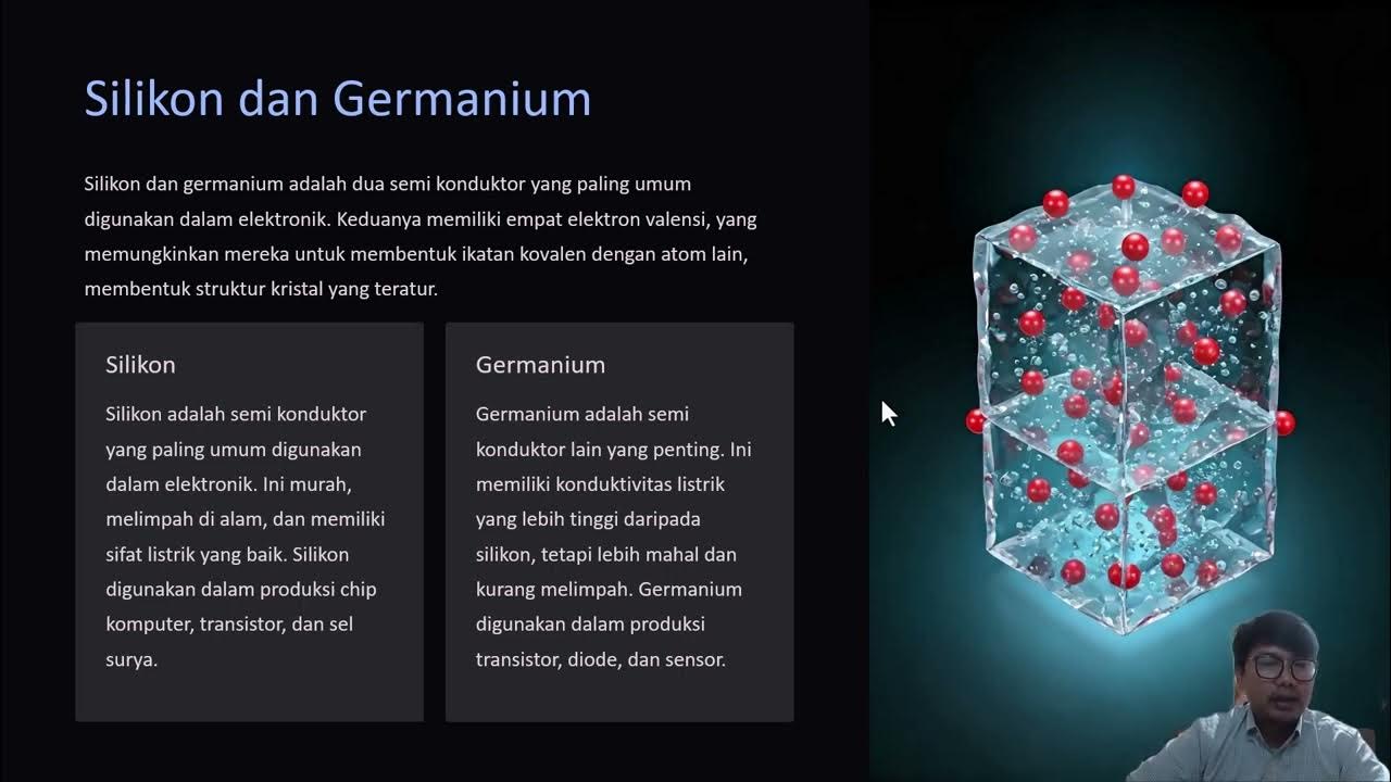
- 💻 Silicon is the most widely used semiconductor material, followed by gallium arsenide.
- 🌡️ Germanium was initially used in semiconductors but was phased out due to its instability at high temperatures.
- ⚡ In intrinsic semiconductors, free electrons and holes are generated when thermal energy allows electrons to move from the valence band to the conduction band.
- 🔧 Doping a semiconductor by adding impurities increases its conductivity by introducing more current carriers like free electrons or holes.
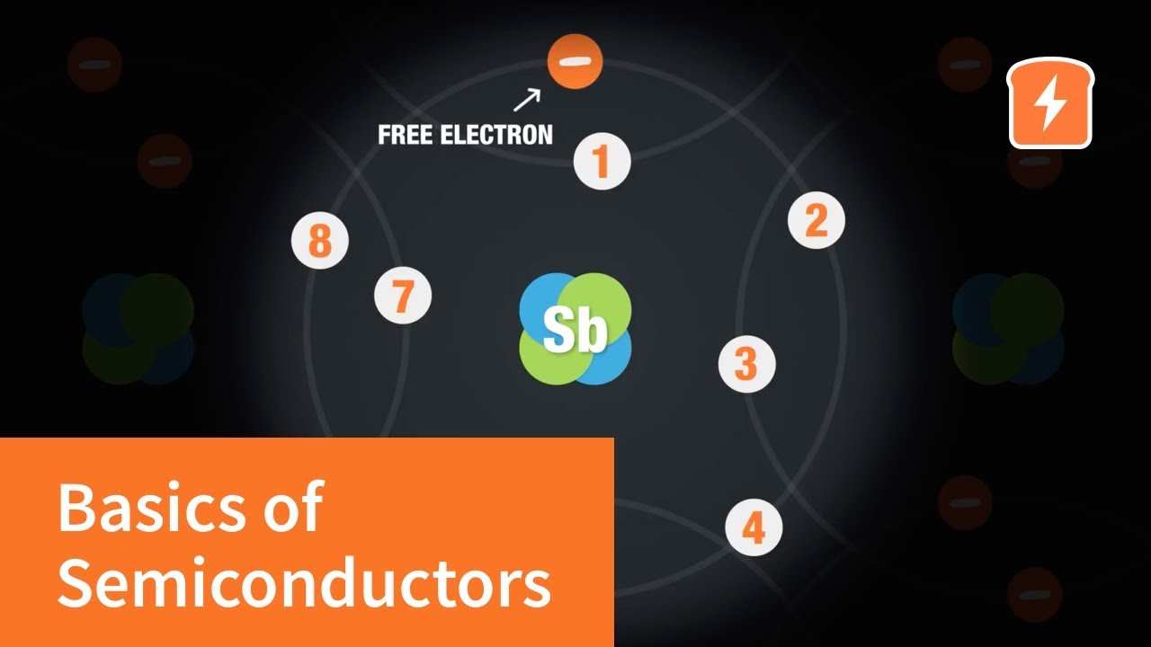
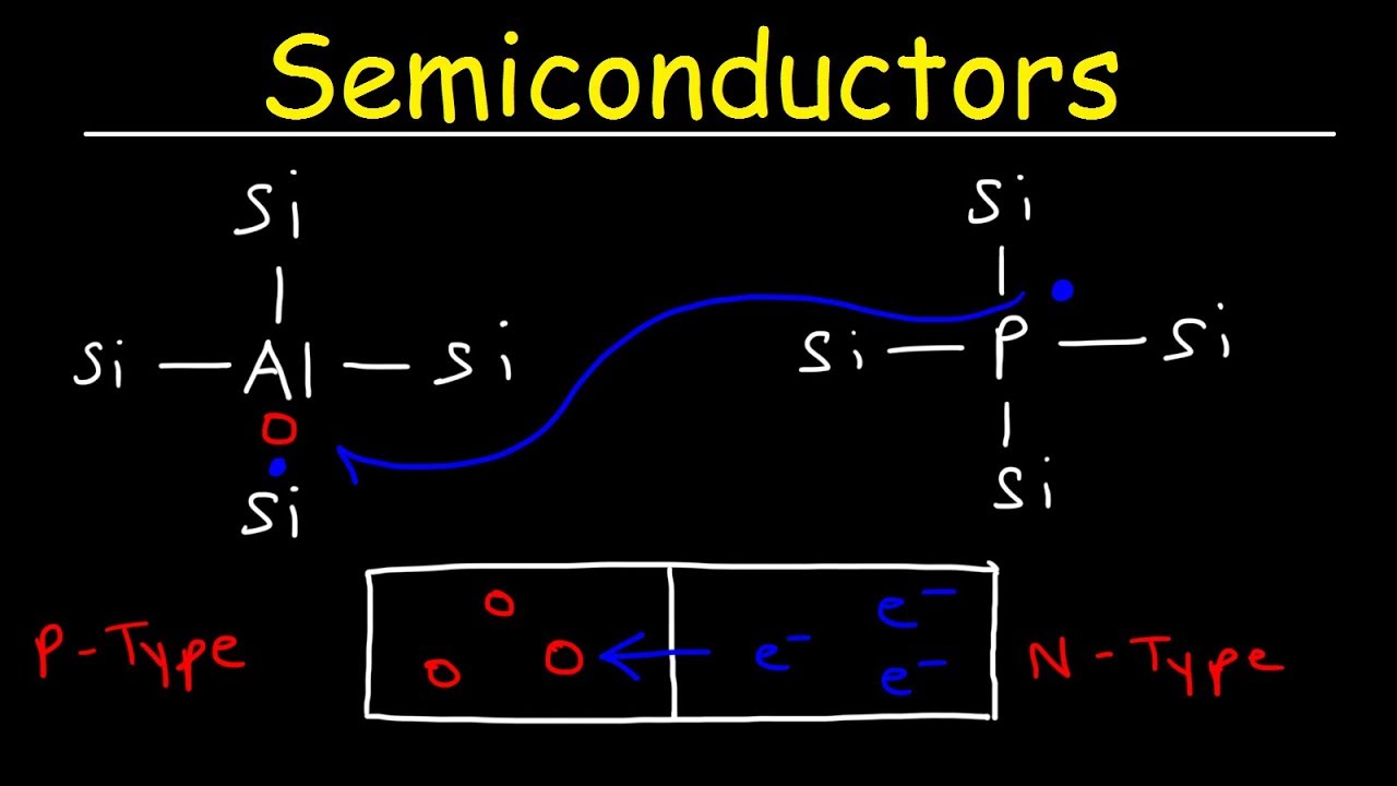
- ⚙️ N-type semiconductors are created by doping with pentavalent atoms, which increase free electrons as the primary current carriers.
- 🔨 P-type semiconductors are made by doping with trivalent atoms, which increase the number of holes as the primary current carriers.
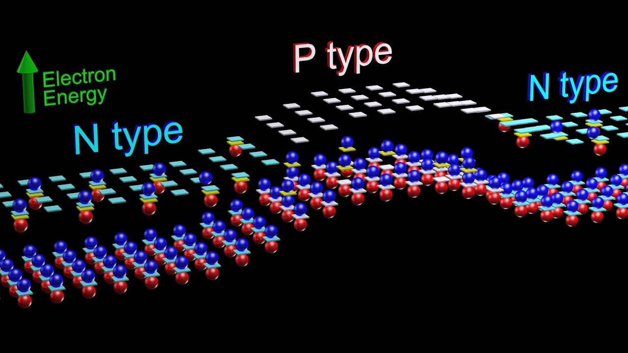
- 🔗 The p-n junction, formed where p-type and n-type semiconductors meet, is the foundation for semiconductor devices like diodes, transistors, and thyristors.
Q & A
What were the limitations of vacuum tubes that led to the development of semiconductor devices?
-Vacuum tubes were bulky, required high operating voltage, and were inefficient, which led to the development of semiconductor devices like transistors.
What are semiconductors and why are they important in electronics?
-Semiconductors are materials that have conductivity between conductors and insulators, making them ideal for controlling electrical current in electronic devices.
What are the most commonly used semiconductor materials in the electronics industry?
-The most commonly used semiconductor materials are silicon and gallium arsenide. Germanium was used in the early years but became less popular due to its instability at high temperatures.
What are free electrons and holes in a semiconductor material?
-Free electrons are negatively charged particles in the conduction band, while holes are positive vacancies left in the valence band when electrons move to the conduction band.
Why do intrinsic semiconductors have poor conductivity?
-Intrinsic semiconductors have poor conductivity because they have a limited number of free electrons and holes, which restricts the flow of current.
How does doping improve the conductivity of a semiconductor?
-Doping improves conductivity by adding impurities to an intrinsic semiconductor, increasing the number of free electrons or holes, which enhances the flow of current.
What is an n-type semiconductor?
-An n-type semiconductor is created by doping an intrinsic semiconductor with pentavalent atoms, which increases the number of free electrons and enhances conductivity.
What is a p-type semiconductor and how is it created?
-A p-type semiconductor is formed by doping an intrinsic semiconductor with trivalent atoms, which increases the number of holes and improves its conductivity.
What is a p-n junction, and why is it important in semiconductor devices?
-A p-n junction is the boundary where p-type and n-type materials meet. It is crucial because it forms the basis for devices like diodes, transistors, and thyristors.
What role do semiconductors play in modern electronic devices?
-Semiconductors are essential in modern electronics, enabling devices like transistors, diodes, and integrated circuits, which are used for signal amplification, switching, and power regulation.
Outlines
💡 Introduction to Semiconductors and Electronics Evolution
This paragraph introduces semiconductors, their role in electronics, and how they replaced vacuum tubes. It explains the limitations of vacuum tubes such as bulkiness and inefficiency, and highlights the importance of semiconductor materials like silicon and gallium arsenide. Semiconductors sit between conductors and insulators in their ability to conduct electricity, which is crucial for their function in electronics.
🔬 The Role of Free Electrons and Holes in Semiconductors
The focus here is on the concept of free electrons and holes in intrinsic semiconductor materials. When thermal energy allows valence electrons to move to the conduction band, it creates free electrons and corresponding vacancies, or holes. These are the two primary current carriers in a semiconductor. However, in their pure, undoped state, semiconductors don’t conduct electricity well due to the limited number of free electrons and holes.
⚙️ Doping: Enhancing Semiconductor Conductivity
This paragraph introduces the concept of doping, which increases the conductivity of a semiconductor by adding impurities. It explains how pentavalent impurity atoms (such as arsenic or phosphorus) with five valence electrons can be added to increase the number of free electrons, thereby enhancing conductivity. The detailed process of adding a phosphorus atom to silicon is visualized, showing how the extra electron becomes free as the temperature rises.
🔋 N-Type Semiconductors and Pentavalent Doping
Here, the focus shifts to n-type semiconductors, where doping with pentavalent atoms increases the number of free electrons. These electrons serve as the primary current carriers, making n-type semiconductors essential for electronic conductivity. The paragraph emphasizes how pentavalent atoms, such as arsenic and phosphorus, create an abundance of free electrons.
🔌 P-Type Semiconductors and Trivalent Doping
The paragraph explains how doping with trivalent impurity atoms (such as boron or gallium) increases the number of holes in a semiconductor, creating p-type semiconductors. Trivalent atoms, with three valence electrons, form incomplete bonds with adjacent silicon atoms, leading to holes that serve as the primary current carriers.
🔗 Formation of P-N Junctions
This paragraph discusses the creation of a p-n junction by doping an intrinsic semiconductor with p-type and n-type materials side by side. The p-n junction is fundamental to modern semiconductor devices like diodes and transistors, forming the basis for many electronic components used today.
📚 Summary and Key Takeaways
In the final paragraph, the key topics discussed in the video are summarized. It recaps the basics of semiconductors, the concept of intrinsic semiconductors and their poor conductivity, and how doping enhances conductivity. The p-n junction, which forms the basis of many semiconductor devices, is highlighted as a critical development in the field of electronics.
Mindmap
Keywords
💡Semiconductors
💡Vacuum Tubes
💡Doping
💡Intrinsic Semiconductor
💡Extrinsic Semiconductor
💡N-type Semiconductor
💡P-type Semiconductor
💡P-N Junction
💡Free Electrons
💡Holes
Highlights
Vacuum tubes were the primary devices for signal amplification and switching before the invention of semiconductors.
Semiconductors are materials that have properties between conductors and insulators, explaining their role in electrical conductivity.
Silicon is the most commonly used semiconductor material in the electronics industry, followed by gallium arsenide.
Germanium, an earlier semiconductor material, is unstable at high temperatures, leading to silicon becoming the preferred material.
Semiconductor materials have two types of current carriers: free electrons and holes.
In intrinsic semiconductors, free electrons are created when thermal energy allows valence electrons to move to the conduction band.
Holes are created when valence electrons jump to the conduction band, leaving vacancies in the valence band.
Doping is a process used to increase the conductivity of a semiconductor by adding impurities, enhancing the number of free electrons or holes.
Pentavalent impurity atoms like phosphorus are added to increase free electrons in an n-type semiconductor.
Trivalent impurity atoms like boron are added to create holes in a p-type semiconductor.
In p-type semiconductors, boron atoms bond with silicon, but the incomplete fourth bond leads to hole creation as an adjacent atom donates an electron.
The boundary between p-type and n-type semiconductor materials is known as a p-n junction, which is the foundation of devices like diodes and transistors.
Doping converts intrinsic semiconductor materials into extrinsic ones, forming either n-type or p-type semiconductors.
Semiconductor devices such as diodes, transistors, and thyristors are based on the p-n junction.
The video explains the basics of semiconductors, the impact of doping, and the formation of p-n junctions, which are critical for modern electronics.
Transcripts
Today, we are going to discuss the basics of semiconductors and their role in the field
of electronics.
Before semiconductor devices existed, vacuum tubes were the only devices available for
signal amplification, switching, and other applications.
Though vacuum tubes are functional, they are bulky, require a high operating voltage, and
are inefficient.
When semiconductor devices like transistors were invented, semiconductors started to acquire
a dominating role in electronics.
Semiconductors are materials that are in between conductors and insulators when it comes to
the ability to conduct electrical current, which explains the name.
The most commonly used semiconductor material in the electronics industry is silicon.
After that, it’s a compound known as gallium arsenide.
Though germanium was used extensively in the early years of semiconductor technology, it
is unstable at high temperatures, so silicon became more widely used.
Semiconductor materials have two current carriers, free electrons and holes.
In an intrinsic semiconductor material, free electrons are produced when the material receives
sufficient thermal energy that provides valence electrons from the valence band enough energy
to jump to the conduction band and turn into free electrons.
When valence electrons jump to the conduction band, they leave vacancies in the valence
band.
These vacancies are called holes.
The number of holes in the valence band is just equal to the number of free electrons
in the conduction band in this undoped, intrinsic material.
A semiconductor material becomes a useful electronic component by controlling its conductivity.
However, semiconductor materials, in their intrinsic state, do not conduct current well.
This is because of the limited number of free electrons and holes in it.
But through a process known as doping, the conductivity of a semiconductor can be increased.
Doping increases the number of current carriers by adding impurities with either more free
electrons or holes to the intrinsic semiconductor material.
The number of free electrons in an intrinsic semiconductor material with four valence electrons,
such as silicon, is increased in the doping process by adding pentavalent impurity atoms,
or atoms with five valence electrons such as arsenic, phosphorus, bismuth, or antimony.[a]
To visualize this, let’s examine a phosphorus atom covalently bonded with four adjacent
silicon atoms.
As we can see, only four valence electrons of the phosphorus atom are used to form covalent
bonds with the silicon atoms, leaving an extra electron.
At lower temperatures, that extra electron stays with the impurity or donor atom but
when the temperature increases, it becomes a free electron.
Once the electron has moved into the conduction band, the dopant atom is now positively charged
as there are more protons in the nucleus than electrons in orbit.
Finally, while the electron is free to move about, the atom itself is fixed in place and
will not move, even with an applied voltage across the material.
[b]So by adding pentavalent impurity atoms to an intrinsic semiconductor material, the
number of free electrons can be increased as well as the conductivity of the semiconductor
material.
Semiconductors doped with pentavalent atoms are n-type semiconductors, since the majority
of its current carriers are electrons.
In order for an intrinsic semiconductor material[c] with four valence electrons, such as silicon,
to have more holes, they are doped with trivalent impurity atoms.
These are atoms with three valence electrons in their valence shell like boron, indium,
and gallium.
To understand how trivalent impurity atoms increase the number of holes in an intrinsic
semiconductor material, let’s see a boron atom attempt to form covalent bonds with the
four adjacent silicon atoms.[d] In this case, at lower temperatures, when the boron covalently
bonds with its neighbors, the fourth silicon atom doesn’t make a bond.
As the temperature increases, an adjacent silicon atom donates an electron to complete
the fourth bond between the boron and the silicon atoms.
There is now a hole where the adjacent silicon atom gave up its electron and the boron atom
is negatively charged as it has an additional electron.
In this case, we can say that by adding more trivalent impurity atoms to an intrinsic semiconductor
material, it increases the number of holes and improves the conductivity of the semiconductor
material.
Semiconductors doped with trivalent atoms are p-type semiconductors since the majority
of its current carriers are holes.
The doping process converts an intrinsic semiconductor material into extrinsic and produces either
an n-type or a p-type semiconductor material.
When you dope an intrinsic semiconductor p-type and then, directly adjacent to that, n-type,
the boundary where the p-type and n-type doped material touches is known as a p-n junction.
[e]This p-n junction is the basis for different semiconductor devices widely used today like
diodes, transistors, and thyristors.
In this video, we talked about the basics of semiconductors, the intrinsic semiconductor
and its poor conductivity, how doping increases the number of current carriers in a semiconductor
material and improves its conductivity.[f] We also briefly mentioned how different semiconductor
devices were created based on the p-n junction.
If you have any questions, leave it in the comments below and if you’ve found this
interesting or helpful, please subscribe to our channel and like this video!
Voir Plus de Vidéos Connexes
How do semiconductors work? (with animation) | Intermediate Electronics
Pengantar Semi Konduktor
Types of Semiconductor Materials | Intrinsic & Extrinsic Semiconductor | Engineering Funda
SEMICONDUCTOR | what is SEMICONDUCTOR | css general science and ability | by ibrar ahmad
Transistors, How do they work?
What Is A Semiconductor?
5.0 / 5 (0 votes)