Beginilah Proses Pembuatan Procesor Yang Rumit
Summary
TLDRThis video delves into the fascinating process of semiconductor manufacturing, focusing on how Intel creates its processors. Starting with raw sand containing high levels of silicon, the video walks through the meticulous stages of silicon purification, crystallization, wafer cutting, and photolithography. Key steps like doping, electroplating copper, and transistor formation are highlighted, showcasing the complexity behind the creation of a microprocessor. The video also touches on the testing phase and explains the significance of CPU architecture in processor functionality. Ultimately, it emphasizes the precision and intricacy involved in making the world's most advanced manufacturing products.
Takeaways
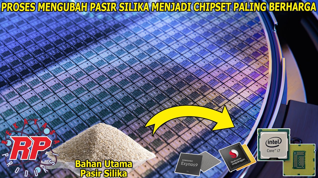
- 😀 Silicon, the primary material for processor manufacturing, is extracted from sand, which contains 25% silicon and is abundant in the Earth's crust.
- 😀 Silicon undergoes purification and refining to become high-purity, electronic-grade silicon for manufacturing semiconductors.
- 😀 Monocrystalline silicon is created by melting and crystallizing purified silicon, and it is used to make wafers, which are the base for processor fabrication.
- 😀 Silicon wafers are sliced into thin discs and polished to a smooth surface to prepare them for the next stages of processor manufacturing.
- 😀 Intel does not manufacture its own silicon wafers but buys them from third-party suppliers, focusing on producing the chips from these wafers.
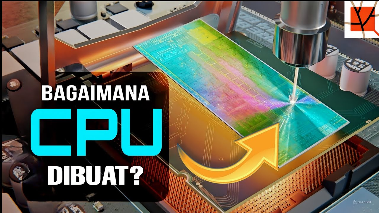
- 😀 Photoresist is applied to the wafer, which is then exposed to ultraviolet (UV) light through a mask to create patterns that define the processor's circuits.
- 😀 The wafer undergoes a process called doping, where ions are implanted into it to change its chemical properties and control the flow of electricity.
- 😀 Electroplating is used to deposit copper onto the wafer to create thin, conductive paths that connect transistors and form the processor's circuitry.
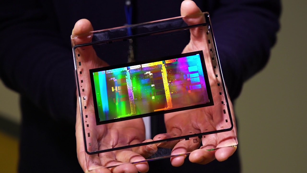
- 😀 A processor consists of multiple layers, often over 20, which include transistors and interconnections built through repeated photolithography and doping steps.
- 😀 The completed wafers are tested for functionality, and any defective processors are discarded while functional ones are used in final processor production.
- 😀 Once functional, processors undergo final testing to measure key attributes such as power dissipation and frequency, and are then categorized and sold according to their specifications.
Q & A
What is the raw material used to make a microprocessor?
-The raw material used to make a microprocessor is sand, which contains 25% silicon. Silicon is the primary element used in processor manufacturing.
What is the role of silicon in processor manufacturing?
-Silicon is essential in processor manufacturing because it serves as the base material for semiconductors. It undergoes a purification process to create high-quality silicon, necessary for building microprocessors.
How is silicon purified to meet manufacturing standards?
-Silicon is purified through several stages to achieve *electronic-grade silicon*, with a purity level that allows for minimal impurities—one or fewer silicon atoms per billion atoms.
What is the process of monocrystal silicon growth?
-Silicon is melted and crystallized to grow a large, single crystal known as monocrystal silicon. This crystal, weighing about 100 kg, is used as the base for creating silicon wafers.
What happens during the wafer production phase?
-In wafer production, the monocrystal silicon ingot is sliced into thin discs, called wafers. These wafers, typically 300 mm in diameter, are then polished to create a smooth, flawless surface.
Why is a photoresist layer applied to the silicon wafer?
-A photoresist layer is applied to the silicon wafer to create patterns for the CPU circuit. This layer is exposed to ultraviolet (UV) light through a mask, which allows for the creation of precise circuit patterns on the wafer.
What is ion implantation, and why is it important in processor manufacturing?
-Ion implantation is a process where ions are implanted into the silicon wafer to alter its electrical properties. This step is critical for defining how electricity will flow within the processor and enables the control of electrical currents in transistors.
How are the metal connections formed on the wafer?
-Metal connections, usually made of copper, are formed on the wafer through a process called electroplating. This involves depositing metal ions onto the wafer, creating thin, conductive layers that connect the transistors and form the processor's electrical pathways.
What does the term 'doping' refer to in semiconductor manufacturing?
-Doping refers to the process of implanting ions into the silicon wafer to modify its electrical properties. This is done to create regions with different electrical conductivities, which are necessary for the functioning of transistors.
How many layers are typically involved in the construction of a modern microprocessor?
-A modern microprocessor can have over 20 layers. Each layer contains intricate patterns of circuits and transistors, which together form the complex architecture of the CPU.
Outlines

Esta sección está disponible solo para usuarios con suscripción. Por favor, mejora tu plan para acceder a esta parte.
Mejorar ahoraMindmap

Esta sección está disponible solo para usuarios con suscripción. Por favor, mejora tu plan para acceder a esta parte.
Mejorar ahoraKeywords

Esta sección está disponible solo para usuarios con suscripción. Por favor, mejora tu plan para acceder a esta parte.
Mejorar ahoraHighlights

Esta sección está disponible solo para usuarios con suscripción. Por favor, mejora tu plan para acceder a esta parte.
Mejorar ahoraTranscripts

Esta sección está disponible solo para usuarios con suscripción. Por favor, mejora tu plan para acceder a esta parte.
Mejorar ahoraVer Más Videos Relacionados
Intel Mask Operation: An Inside Look at a Critical Manufacturing Step
INTIP PROSES PRODUKSI CHIP SEMIKONDUKTOR TERMODERN DARI SILIKON MURNI KE REVOLUSI DIGITAL PROCESSOR
Bagaimana Microchip Dibuat? || Langkah - Langkah Proses Pembuatan CPU Komputer

Organisasi & Arsitektur Komputer | Nathanael Ferry Pratama | 2021130019

Why Malaysia Failed to Become an Asian Economic Tiger

Massive News For Intel Stock Investors
5.0 / 5 (0 votes)
