How do semiconductors work? (with animation) | Intermediate Electronics
Summary
TLDRThis video explores the fundamentals of semiconductors, highlighting their crucial role in electronics. It contrasts the limitations of early vacuum tubes with the advent of semiconductor devices like transistors, which revolutionized the field. The script delves into the properties of semiconductors, explaining how materials like silicon and gallium arsenide conduct electricity between conductors and insulators. It details the process of doping to enhance conductivity, creating N-type and P-type semiconductors, and introduces the P-N junction as the foundation for devices such as diodes and transistors. The video concludes by inviting viewers to engage with the content and subscribe for more informative content.
Takeaways
- 🌐 Vacuum tubes were the primary devices for signal amplification and switching before semiconductors were invented.
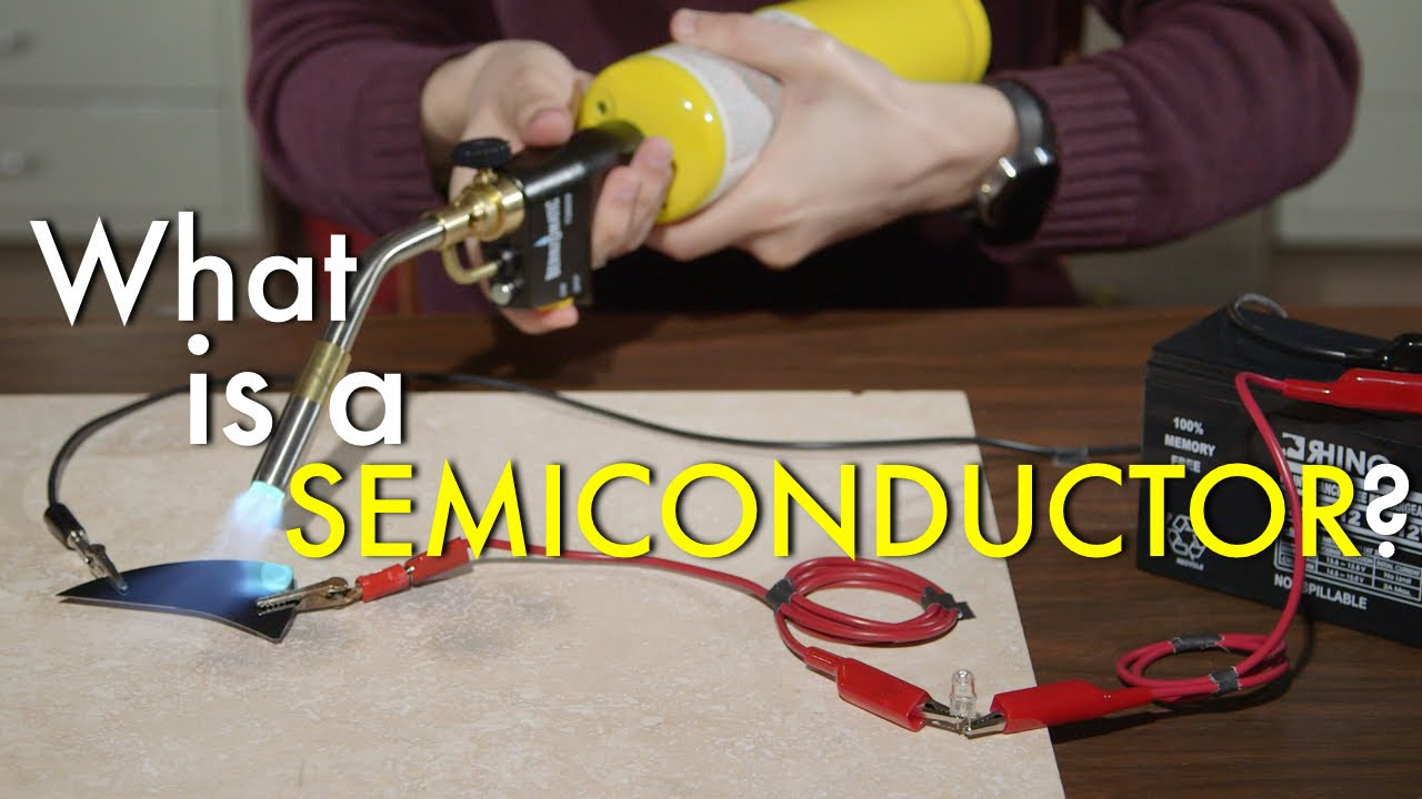
- 🔌 Semiconductors are materials with electrical conductivity between that of conductors and insulators.
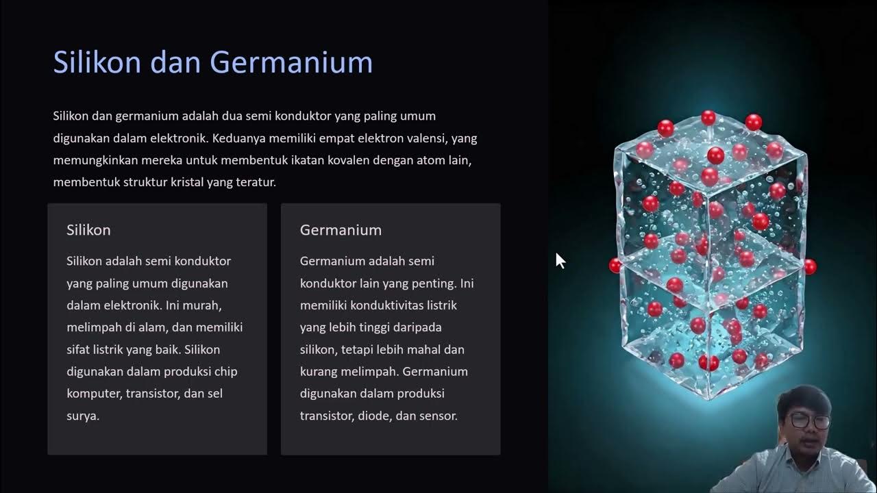
- 💾 Silicon is the most commonly used semiconductor material in the electronics industry, followed by gallium arsenide.
- 🔋 Semiconductors have two types of current carriers: free electrons and holes, which are crucial for their operation.
- 🔥 Intrinsic semiconductors have a limited number of free electrons and holes, resulting in poor conductivity.
- 💡 Doping is the process of adding impurities to increase the number of current carriers and improve conductivity in semiconductors.
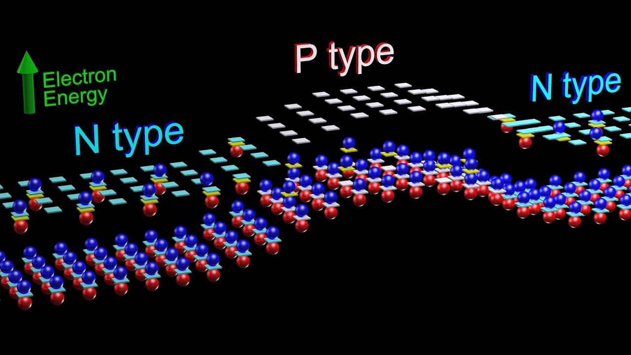
- 📍 Pentavalent impurities, such as arsenic, phosphorus, bismuth, or antimony, increase the number of free electrons, creating N-type semiconductors.
- 📌 Trivalent impurities, like boron, indium, and gallium, increase the number of holes, creating P-type semiconductors.
- 🔄 The P-N junction, formed by combining N-type and P-type semiconductors, is fundamental to many semiconductor devices.
- 🛠️ Devices such as diodes, transistors, and thyristors are based on the P-N junction and have widespread applications.
- 📚 The script provides an educational overview of semiconductor basics, doping, and the significance of the P-N junction in electronic devices.
Q & A
What were the limitations of vacuum tubes in electronics?
-Vacuum tubes were bulky, required a high operating voltage, and were completely inefficient compared to semiconductor devices.
What is a semiconductor and why is it called so?
-A semiconductor is a material with electrical conductivity between that of a conductor and an insulator, hence the name 'semiconductor'.
Which is the most commonly used semiconductor material in the electronics industry?
-Silicon is the most commonly used semiconductor material in the electronics industry.
What are the two types of current carriers in semiconductor materials?
-The two types of current carriers in semiconductor materials are free electrons and holes.
How are free electrons produced in an intrinsic semiconductor material?
-Free electrons are produced when the material receives sufficient thermal energy, allowing valence electrons to jump from the valence band to the conduction band.
What are holes and how are they related to free electrons in an intrinsic semiconductor?
-Holes are vacancies left in the valence band when valence electrons jump to the conduction band. The number of holes is equal to the number of free electrons in an intrinsic semiconductor.
How does doping increase the conductivity of a semiconductor material?
-Doping increases the conductivity of a semiconductor by adding impurities that provide more free electrons or holes to the intrinsic semiconductor material.
What are pentavalent impurity atoms and how do they affect the number of free electrons in a semiconductor?
-Pentavalent impurity atoms, such as arsenic, phosphorus, bismuth, or antimony, have five valence electrons and when added to a semiconductor, they contribute an extra electron, increasing the number of free electrons and the material's conductivity.
What type of semiconductor is created when pentavalent impurity atoms are added?
-Semiconductors doped with pentavalent atoms are N-type semiconductors, characterized by an excess of free electrons as the majority of current carriers.
What are trivalent impurity atoms and how do they increase the number of holes in a semiconductor?
-Trivalent impurity atoms, such as boron, indium, and gallium, have three valence electrons. When they replace atoms in the semiconductor, they create holes, thus increasing the number of holes and the material's conductivity.
What is the result of combining N-type and P-type semiconductor materials?
-Combining N-type and P-type semiconductor materials creates a P-N junction, which is the basis for various semiconductor devices such as diodes, transistors, and thyristors.
What is the significance of the P-N junction in semiconductor devices?
-The P-N junction is significant as it forms the foundation for the operation of many semiconductor devices, allowing for the control of electrical current and the creation of various electronic components.
Outlines

Dieser Bereich ist nur für Premium-Benutzer verfügbar. Bitte führen Sie ein Upgrade durch, um auf diesen Abschnitt zuzugreifen.
Upgrade durchführenMindmap

Dieser Bereich ist nur für Premium-Benutzer verfügbar. Bitte führen Sie ein Upgrade durch, um auf diesen Abschnitt zuzugreifen.
Upgrade durchführenKeywords

Dieser Bereich ist nur für Premium-Benutzer verfügbar. Bitte führen Sie ein Upgrade durch, um auf diesen Abschnitt zuzugreifen.
Upgrade durchführenHighlights

Dieser Bereich ist nur für Premium-Benutzer verfügbar. Bitte führen Sie ein Upgrade durch, um auf diesen Abschnitt zuzugreifen.
Upgrade durchführenTranscripts

Dieser Bereich ist nur für Premium-Benutzer verfügbar. Bitte führen Sie ein Upgrade durch, um auf diesen Abschnitt zuzugreifen.
Upgrade durchführenWeitere ähnliche Videos ansehen

Classification of Semiconductors (Intrinsic/Extrinsic, P-Type/N-Type)

Future of Semiconductors: Silicon Carbide & Gallium Nitride as Next-Gen Semiconductors

What Is A Semiconductor?

Pengantar Semi Konduktor

SEMICONDUCTOR | what is SEMICONDUCTOR | css general science and ability | by ibrar ahmad

Semiconductors - Physics inside Transistors and Diodes
5.0 / 5 (0 votes)
