VHDL code for 4 bit ALU and Realization on FPGA development Board
Summary
TLDRIn this instructional video, the presenter guides viewers through the process of designing a 4-bit ALU (Arithmetic Logic Unit) using VHDL code. The tutorial covers understanding ALU's logical functions and boolean expressions, creating an Xilinx ISE project, coding, simulating, synthesizing, and generating a bit file for FPGA implementation. The presenter also demonstrates how to create a UCF file for pin constraints and uses an FPGA programmer to load the ALU functionality onto the board, testing it with switches and LEDs to verify the operations.
Takeaways
- 😀 The video is a tutorial on designing a 4-bit ALU (Arithmetic Logic Unit) using VHDL and implementing it on an FPGA development board.
- 🔍 The presenter starts by explaining the logical functions and boolean expressions of the ALU before writing the VHDL code.
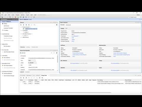
- 💻 The tutorial involves creating a project in Xilinx ISE, writing VHDL code for the 4-bit ALU, simulating the code, and synthesizing it.
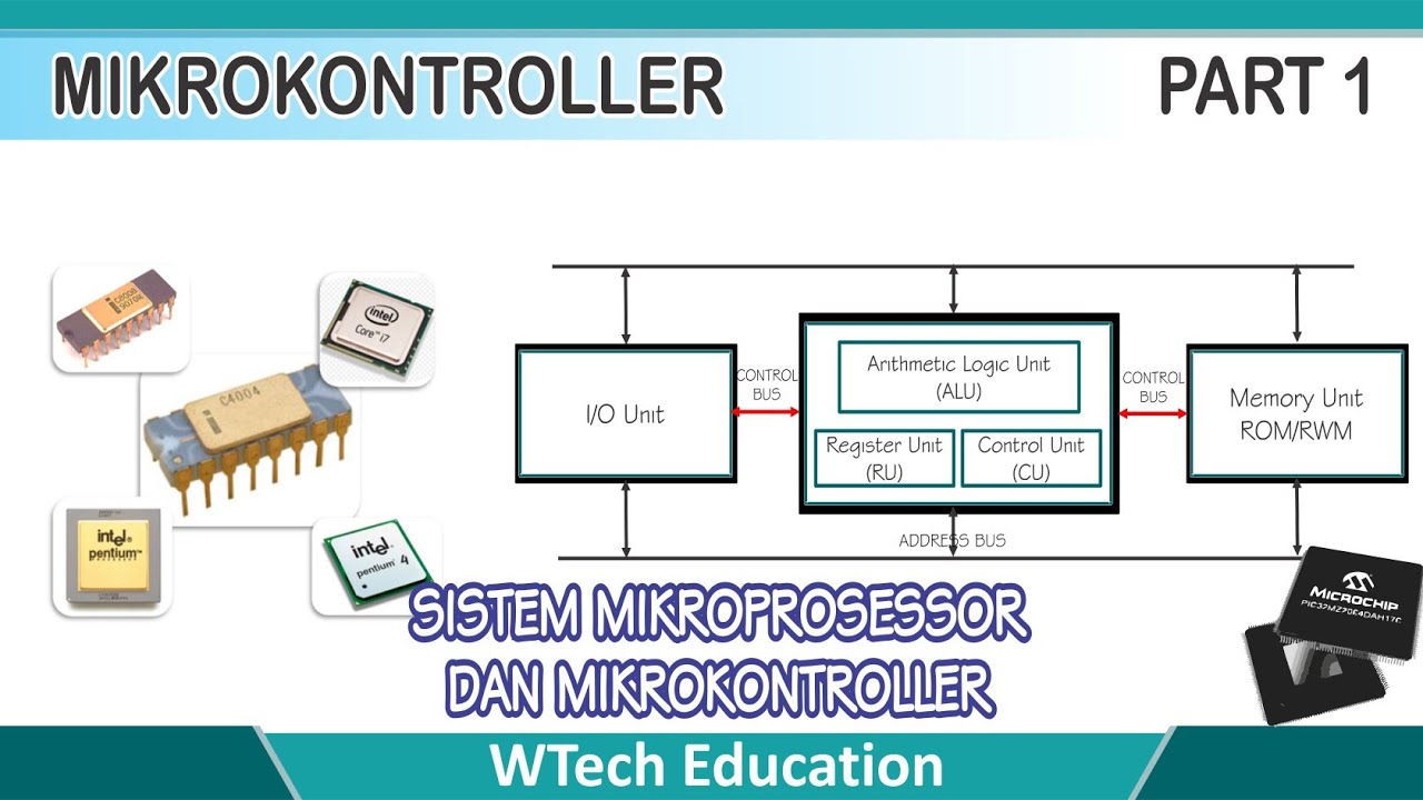
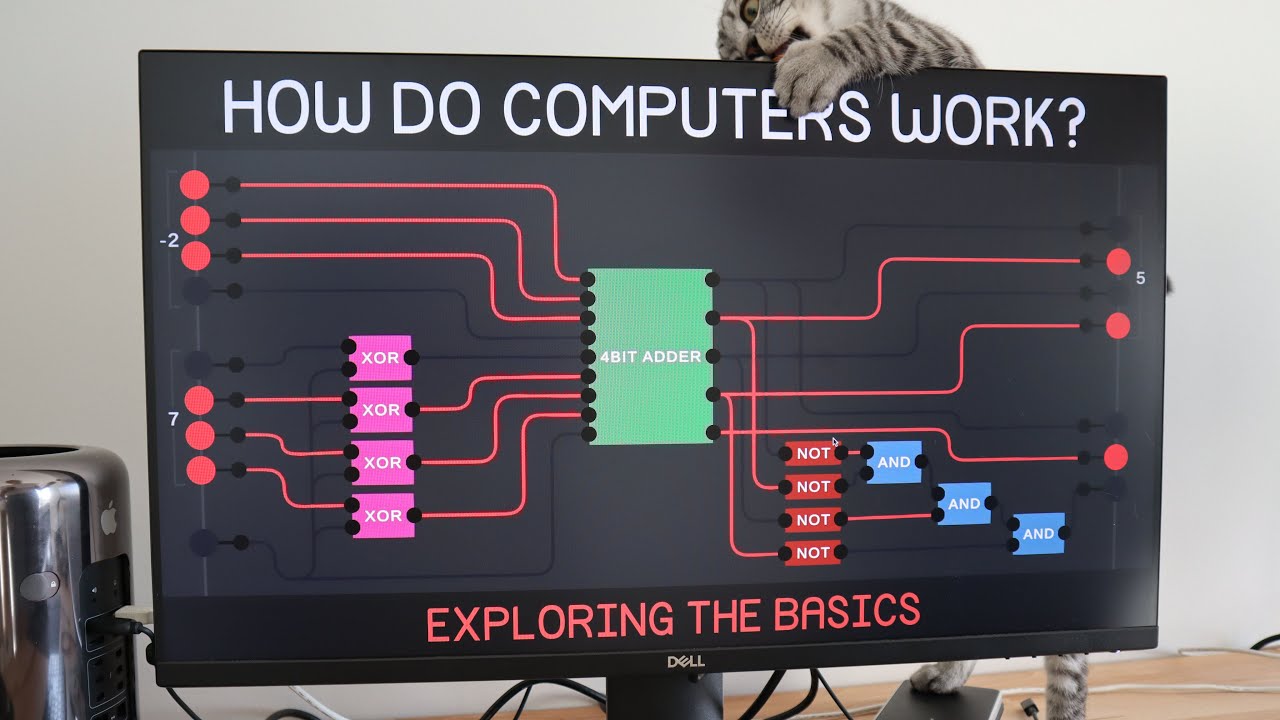
- 📈 The ALU performs various operations based on the select line inputs, including addition, subtraction, AND, NAND, XOR, XNOR, OR, and passing through the input A.
- 🔢 The inputs to the ALU consist of two 4-bit inputs (A and B) and a 3-bit select line, with the output being a 4-bit ALU result.
- 📝 The VHDL code uses a 'with select' statement to handle different operations based on the select line values.
- 🔩 The synthesis process involves implementing the ALU using components like adders, subtractors, and multiplexers.
- 🖥️ The video demonstrates a simulation of the ALU to verify its functionality for different select line inputs and operations.
- 🔌 A UCF (User Constraint File) is created to define pin connections for the FPGA implementation, specifying the physical connections for inputs, outputs, and select lines.
- 💾 The final step involves generating a bit file, programming the FPGA board, and testing the ALU functionality using switches and LEDs on the board.
Q & A
What is the main topic of the video session?
-The main topic of the video session is to write VHDL code for a 4-bit ALU (Arithmetic Logic Unit) and its implementation on an FPGA development board.
What are the logical functions and boolean expressions needed to understand before writing the VHDL code for the ALU?
-Before writing the VHDL code, one must understand the logical functions such as addition, subtraction, AND, OR, XOR, and NAND operations, as well as the boolean expressions that represent these functions in the ALU design.
What is the purpose of the select line in the 4-bit ALU design?
-The select line in the 4-bit ALU design is used to choose between different operations such as addition, subtraction, AND, OR, XOR, and other functions based on the combination of bits set on the select line.
How many bits are in the select line for the 4-bit ALU design?
-The select line for the 4-bit ALU design is 3 bits, allowing for eight different combinations of operations.
What is the process of implementing the VHDL code on the FPGA development board?
-The process involves writing the VHDL code, creating a project in Xilinx ISE, simulating the code, synthesizing it, creating a UCF file, generating a bit file, and then implementing the bit file on the FPGA development board.
What is a UCF file used for in the context of FPGA implementation?
-A UCF (User Constraint File) is used to define pin connections between the FPGA and external components, specifying the physical pins to which the signals in the VHDL code are assigned.
How many different operations can be performed with the 4-bit ALU design as described in the script?
-With the 3-bit select line, the 4-bit ALU design can perform eight different operations, each corresponding to a unique combination of the select line bits.
What is the significance of the 'others' clause in the VHDL code for the ALU?
-The 'others' clause in the VHDL code for the ALU is used to handle any remaining cases that are not explicitly covered by the select statements, ensuring that all possible input combinations are accounted for.
What are the steps involved in testing the ALU functionality on the FPGA board?
-The steps include loading the bit file onto the FPGA, connecting the select lines and input switches to the appropriate pins on the FPGA, and observing the LED outputs to verify that the ALU performs the expected operations based on the selected operation.
How does the video script guide the user to verify the simulation of the ALU operations?
-The script guides the user to verify the simulation by providing examples of input values for A and B, and the expected results for each operation based on the select line settings. It also demonstrates how to force values in the simulation and observe the outputs to confirm the correctness of the ALU operations.
Outlines
📝 Introduction to 4-bit ALU VHDL Coding
This paragraph introduces the session on writing VHDL code for a 4-bit Arithmetic and Logic Unit (ALU) and its implementation on an FPGA development board. The speaker outlines the process, which includes understanding logical functions and boolean expressions, creating an Xilinx ISE project, writing VHDL code for the ALU, simulating, synthesizing, creating a UCF file, generating a bit file, and implementing it on the development board. The ALU design involves two 4-bit inputs, a select line, and a 4-bit output with various operations based on the select line combinations.
🔍 Detailed Explanation of ALU Operations and VHDL Code Writing
The speaker provides a detailed explanation of the ALU operations and the process of writing VHDL code. The ALU performs different operations based on the select line inputs, such as addition, subtraction, AND, NAND, XOR, XNOR, and OR. The VHDL code includes declarations of inputs and outputs, use of the 'with-select' statement for conditional operations, and the implementation of arithmetic and logical operations using standard VHDL constructs. The paragraph also covers the syntax checking and synthesis process to ensure the code is correctly translated into hardware components.
🔬 Simulation and UCF File Creation for FPGA Implementation
This paragraph discusses the simulation of the ALU to verify its functionality with different input values and select line combinations. The speaker demonstrates the simulation process, showing how the ALU performs addition, subtraction, and logical operations. Following the simulation, the speaker explains the creation of a UCF (User Constraint File) necessary for mapping the VHDL code to the physical pins of the FPGA. The UCF file specifies the pin connections for the select lines, input A and B, and the ALU output.
🚀 Finalizing FPGA Programming and Testing ALU Functionality
The final paragraph covers the steps to program the FPGA using the generated bit file and testing the ALU functionality. The speaker guides through opening the programmer, selecting the appropriate FPGA family and COM port, and programming the FPGA board. After programming, the speaker describes how to test the ALU by connecting switches to the select lines and input A and B, and observing the output on LEDs. The goal is to verify that the ALU performs the correct operations as per the select line settings.
Mindmap
Keywords
💡VHDL
💡ALU
💡FPGA Development Board
💡Boolean Expressions
💡Select Line
💡Simulation
💡Synthesis
💡UCF File
💡Bit File
💡Implementation
Highlights
Introduction to a VHDL code design course for a 4-bit ALU and its FPGA implementation.
Understanding the logical functions and Boolean expressions of a 4-bit ALU before coding.
Creating a Xilinx ISE project for 4-bit ALU coding using VHDL.
Process of simulation, synthesis, and bit file generation for FPGA implementation.
Description of a 4-bit ALU design with two 4-bit inputs and a 4-bit output.
Eight different combinations of operations for the ALU using a 3-bit select line.
Explanation of the ALU operation when the select line is set to zero for addition.
Demonstration of subtraction operation with the select line set to 001.
Illustration of the AND operation when the select line is 010.
NAND operation explanation with the select line set to 011.
XOR and XNOR operations explained for select line values of 100 and 101.
OR operation demonstration for a select line value of 110.
Pass-through functionality of the ALU for a select line value of 111.
Writing of VHDL code for the 4-bit ALU with input declarations and entity definition.
Use of a with-select statement to write the ALU program in VHDL.
Synthesis of the VHDL code to verify the implementation of ALU operations.
Simulation of the ALU to test various operations and validate the design.
Generation of a UCF file for pin constraints and FPGA board implementation.
Programming the FPGA board with the bit file and testing the ALU functionality.
Transcripts
[Music]
hello friends welcome to the village
design course
so in today's session we are going to
write a vhdl
code for 4-bit aou and its relation
realization on the fpga development
board
[Music]
so before starting writing a vhdl code
first of all we have to understand its
logical functions then its boolean
expressions
then we are going to create a vhdl
um xilinx isc project where we are going
to write a
4 bit alu coding using a vhdm
then we are going to do the simulation
then synthesis
creating a ucf file generate a bit file
and that bit file you are going to
implement on the
development board so let's start so
this this is a four bit aou uh design i
have taken
so in this in this we have four bit
input four bit out uh so so we have two
four bit input a is a four bit
b also four bit and
alu out is also four bit so
and these are the various combinations
or operations we are going to do
using alu so we have taken
eight different combinations so for that
we need a select line so again select
line is again a three bit
input so totally we have
three inputs and one output so out of
these three input
input a b are four bit and select line
as a three bit
so how it how it works when select line
is zero zero
we are going to do the operation of a
plus b
we are going to do the operation of a
plus b
and that is going to the output alu out
when select line is zero
zero 1 what we are doing we are doing a
minus
b a minus b then
when select line is equal to 0 1 0 we
are doing a
and b then if it is a 0 1 1 a
nand b one zero zero then a xor b
one zero one a x nor b where it is one
one zero
a or b and finally if it is a one one
one we are passing whatever input of
a bit uh a four bit you are passing to
the output
a load so for this function for this
function
now we are going to write a vhdl vhdl
code okay so let's let's begin to write
a vhdl code
so open the isc create a new project
file new project
so we are going to write a l u 4
b ok so i am creating a project alu 4
bit
next so these these parameters are
exactly same because it is already one
time we have saved
so for our family is spartan 3 xc3s 58
tq144
next finish
now we have to add a new source so vhdl
module
vsdn module a l you
underscore for underscore bit okay
so we are going to write vhdl code for
four bit alu so as i said as i said
how many inputs we have we have input a
b which are four bit
so let us declare it a comma b
r of type in bus and total four bits
means three down to
zero then we have another input select
line
that is also an in with a bus of three
bits so it is
two down to zero and we have output alu
underscore
out this is the output
and the bus width is three down to zero
so that is a four bit
okay so this much declarations we have
to do
so let's reconfirm a four bit b four bit
select line three bit
alu out 4-bit ali out
ali out for it so let's generate a
entity so here we are going to use some
some additional features like additional
subtraction so we need to add a
library called unsign so let's add it
okay done now your entity is also
already declared so library declaration
then entity
port a comma b in 4 bit select line
input 3 bit ali out 4 bit
now here we have to write a program so
we are going to use
we are going to use
we are going to use a with select with
select
uh statement to write to write a
alu program okay
so let's begin let's begin so i am going
to write
with s e l
select this is a concurrent statement
right everyone knows that we have
already seen this
statement syntax and usage so with
scl select now output is a l you
underscore
out is equal to
the first condition is a plus b
so a plus b
when when this straight line is equal to
when it is
0 0 0 right
then we have to know other conditions
also we need to write
when it is 0 0 1 what is the condition
a minus b and
then when 0 1 0 it is a and b 0
1 0 it is
a and b
then it is 0 1
1 when it is 0 it is an and xor xnor
then i am writing here a nand b
then it is when it is one zero zero it
is
for four it is xor
xor yes then
for one zero one it is
x nor
x no right
when it is a six it is a or b
a or b right and it is a final event is
when others clause
so here we are terminating when others
so that means when it is a 1 1
1 we are going to write a right
so this this this completes our program
this completes our program
so we have to check for the syntax let
us check the syntax if any by mystically
we have done any mistake then it will
indicate through an error
okay then do the synthesis
so let's see the synthesis
really four bit so
it is implemented if you see here adder
subtractor
then multiplexer for selection and here
it is implemented using xor
and other functionality and gate
everything it is implemented right
so let us let us let us see the
simulation fastly
and then we will go for generating a bit
file so simulate it
so let's start
so i am giving a value some random value
let us say uh
1 0 1 0 sorry
1 0 1 0 binary apply
ok b
let us take example b is 0
1 0 1 ok for you
then select line let us start with the
initial
so it is 0 0 0 apply ok
and run it ok now if you can see here
so a plus b okay
so 10 plus 5 becomes 15 10 plus 5
becomes 15 if you can see here so
the first operation au operation is when
straight line is 0 0
0 it performs a plus b now if select
line is 0
0 1 it should perform
it should perform 0 0 1 it should
perform a minus b
so 10 minus for you again it should come
five so result should be five got it
got it now if select line is
zero one zero okay zero
one zero okay so it should perform and
operation
so it should perform and operation but
if you see the end operation
so zero it is a bit wise bitwise
operation so zero
and and one it is zero zero
one zero one zero again zero and zero
one again
zero so this is and operation now let us
see the for nand operation
so zero one one if straight line is zero
one one
what is operation as per the select line
is zero 1 1 we have written a code for
nand
so let's simulate it so 9 is invert off
and so whatever here we are getting 0 0
0 it will imply
invert so all are ones now when it is
1 0 0 when it is a fourth condition if
select line is 1
0 0 what is the operation we have
written we have written
for 1 0 0 it is a a x or b so let's
let's do it
so a x or b
ax or b also exactly same because 0 1 1
1 0 1 and 0 1 1 1 0 1 so let us change
some a value and again run it so force
constant
so one one zero zero okay
okay run it now check it now x so zero
zero one zero x or one it is one
zero x xor 0 is 0 1 x or 1 is 0 and 1
x or 0 is 1 so like that like that we
can verify the
simulation like that we can verify the
simulation
so let us let us go ahead with
writing or generating a ucf file so for
that for that what you have to do
why we need to use a file now to
implement this program onto a pc we need
a pin connection
yes so for that pin connections we need
a
ucf generation so let's generate it
right click
new source then you have to select
implement constraint file and this is
a l u dot u c f
okay so i'm going to write a ucl file
next
finish okay so here you say file is
generated
so uh i will use some
already written to shorten our time
okay so for that go back now
now what we are going to use we are
going to use this
these three switches as a select line so
for that select two is a
pin pin location is p8 select one is p3
and select
0 is p5 so just modify it so select
2 is p8
yes select 2 is p8 select off one is p3
and select of zero is p5 it is already
there okay
now for the for the inputs
uh four bit b input and four bit a input
we are going to use this j14 header so a
of a of 0 is connected to p 15
or or we can say the first four switches
are used for
four bit b input and next four bit
four switches are used as a 4-bit a
input so
here 4-bit a so sorry b input
and here is a input so for that b of 3
is equal to p-31
that is the first switch so first switch
represent the msb of b and the fourth
switch represent the
lsb of the b input similarly this fifth
switch will represent as a
msb of a and last switch as a lsb of
b so let's let's do it so b of 3 is
equal to
p 31 so b of 3 already it is p 31 b of 2
is p 32
b of 1 is p 28 v of 0 is p
30 b of 0 is p 30 correct
then a of 3 we have to assign p21 a of 3
p27 sorry p27
then p29 p24 p25 all right
all right now then the ali output we are
going to connect
to the this led output and that is
connected to this p4 port
so for ali out of 3 so that is msb out
is 141
so ale of 3 msb is 141 so i am modifying
here
141 then
second is 140 3
i guess yes 143 138 139
then 138
then 130 right
so this creates our ucf file now we are
ready with the ucf file save it
and let's generate a programming file
okay
so once the programming file is ready
then we
are going to open a pga programmer
and using fpga programmer we are going
to write a
implementer write a bit file onto a pg
and we will check the alu functionality
okay so let's wait for some time
it is generating yes almost regenerated
a bit file
then meanwhile time i will just open the
programmer
so this is the programmer we are using
usually to write a
fpga so for that usually it will show us
the
uh the fpga board family it is xc3s
says and you have to select a com port
so i am using com4
because the usb port i connected to the
fpga is a
com 4 now once this bit file is
generated
through this open file we are going to
open the bit file
so open file so wherever you have
written a code so we have
created a new project that is yearly 4
bit
and you can see here alu 4 bit bit file
is generated
we have to say open and let's say
program
so my fpga started programming
so now we'll move to the fpga board
so yes now if you if you can observe
here if you can observe here
the fpga is program and the led
is blinking over here led is blinking
over here blue led
now we have to see the connections for
the connections
we have used this p6 uh sorry uh p2
header
p2 header for this select line so that i
have to connect to the
j3 header j3 header
once again i will confirm okay so
now our program is ready we are loaded
alu functionality into this fpga
so how we are going to test it so these
are the select lines
select line of three two one sorry
sorry two one zero so three bit select
line
so this first switch will act as a msb
of b input so
b first four switches for the b input
and
second remaining four switches for the a
input
and this first four leds indicates the
alu output okay
so let us make it so if i make it a
is one b is one
so for zero zero it should add so what
is not adding
maybe weight so this is
j3 j3
so let me verify it once again
you
Weitere ähnliche Videos ansehen
Exploring How Computers Work
Sistem Mikroprosesor & Mikrokontroler Part 1
43. OCR A Level (H046-H446) SLR8 - 1.2 Introduction to programming part 4 mathematical operators
PHP For Beginners, Ep 3 - Your First PHP Tag
N bit Multiplier in Verilog (with code)| Verilog Project | Xilinx Vivado | Electronics Project
CANGGIH!!! Cara buat Kunci pintu Pakai PASSWORD
5.0 / 5 (0 votes)