2 Semikonduktor Semikonduktor Tipe P dan N
Summary
TLDRThis video provides a detailed explanation of semiconductors, focusing on their properties, types, and the process of doping. It starts by introducing the concept of semiconductors, comparing them with conductors and insulators. Key materials like silicon and germanium are discussed, with an emphasis on silicon’s widespread use. The video explains doping techniques and how adding impurities like phosphorus and boron creates N-type and P-type semiconductors, respectively. These processes alter electrical properties, enabling their use in various electronic components. The video concludes with insights into the application of semiconductors in technology.
Takeaways
- 😀 Semiconductors are materials with electrical conductivity between conductors and insulators, with silicon and germanium being common examples.
- 😀 Conductors have one valence electron, insulators have eight valence electrons, while semiconductors like silicon have four valence electrons.
- 😀 Silicon is the most popular semiconductor material because it is abundant and can be easily extracted from the Earth.
- 😀 Doping is the process of adding impurities to a semiconductor to change its electrical properties.
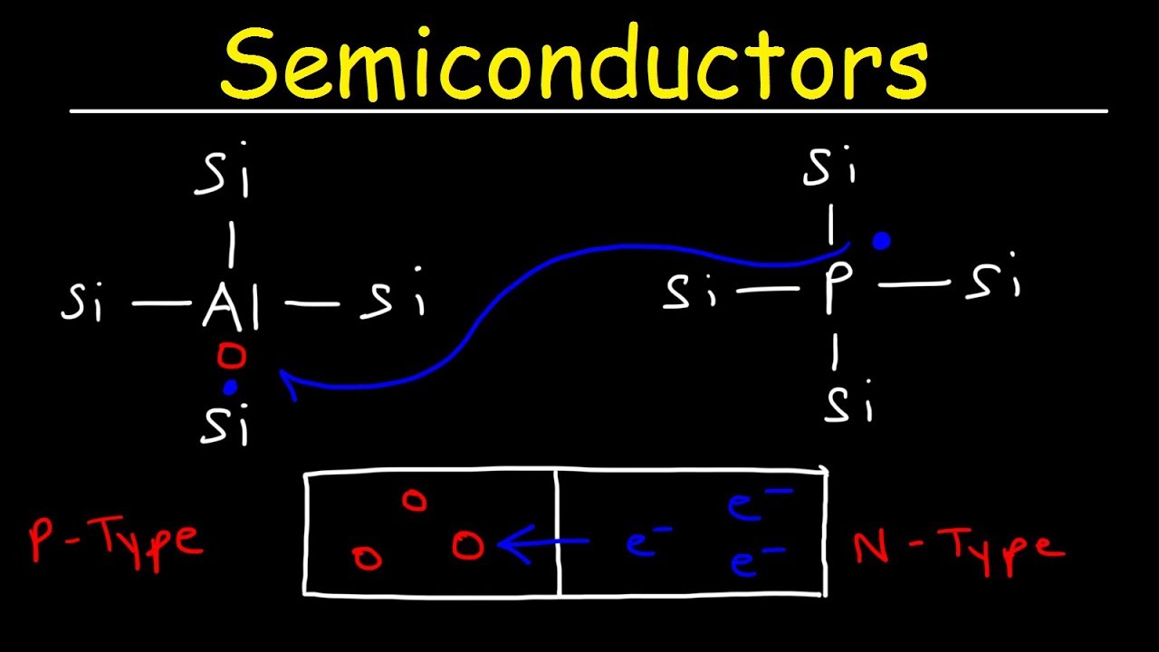
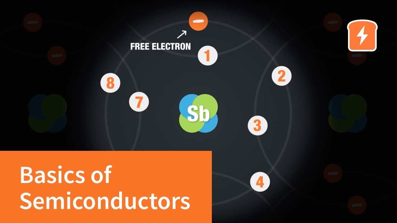
- 😀 N-type semiconductors are created by doping silicon with pentavalent elements like phosphorus, resulting in extra electrons that improve conductivity.
- 😀 P-type semiconductors are created by doping silicon with trivalent elements like boron, resulting in holes (electron deficiencies) that facilitate conductivity.
- 😀 Pentavalent dopants (such as phosphorus) add extra electrons to the silicon, creating an N-type semiconductor.
- 😀 Trivalent dopants (such as boron) create holes by missing one electron, creating a P-type semiconductor.
- 😀 N-type semiconductors are known as donors because they donate extra electrons, while P-type semiconductors are acceptors because they accept electrons.
- 😀 The electrical properties of semiconductors can be dramatically altered with small amounts of dopants, enabling the creation of transistors and other electronic devices.
Q & A
What are semiconductors and why are they important?
-Semiconductors are materials that have properties between those of conductors and insulators. They are essential for electronics because their electrical properties can be manipulated through doping, allowing them to be used in devices like transistors, diodes, and integrated circuits.
What is the difference between conductors, insulators, and semiconductors?
-Conductors have one electron in their outer shell, allowing them to easily conduct electricity. Insulators have eight electrons in their outer shell, making them poor conductors. Semiconductors, like silicon, have four valence electrons, making them neither good conductors nor insulators, but their electrical conductivity can be enhanced by doping.
Why is silicon the most commonly used semiconductor material?
-Silicon is the most widely used semiconductor because it is abundant on Earth, easy to extract, and has favorable electrical properties. Additionally, silicon can be easily processed and doped to modify its electrical conductivity.
What is doping in semiconductor materials?
-Doping is the process of adding small amounts of foreign atoms (impurities) to a semiconductor material, like silicon, to change its electrical properties. This can create n-type or p-type semiconductors, depending on the type of impurity used.
What is the purpose of doping in semiconductors?
-The purpose of doping is to increase the number of free charge carriers (electrons or holes) in a semiconductor, which enhances its ability to conduct electricity. Doping can either add extra electrons (n-type) or create holes that act as positive charge carriers (p-type).
What is the difference between n-type and p-type semiconductors?
-N-type semiconductors are created by doping silicon with elements that have five valence electrons (like phosphorus), which adds extra electrons. P-type semiconductors are created by doping silicon with elements that have three valence electrons (like boron), creating 'holes' where electrons are missing.
What happens when silicon is doped with phosphorus?
-When silicon is doped with phosphorus, which has five valence electrons, it introduces extra electrons into the material. This creates an n-type semiconductor, where the free electrons are the majority charge carriers.
What happens when silicon is doped with boron?
-When silicon is doped with boron, which has three valence electrons, it creates holes in the crystal structure, leading to a p-type semiconductor. These holes act as positive charge carriers, and they can attract electrons to move through the material.
What is the role of impurities like arsenic and aluminum in doping?
-Impurities like arsenic (pentavalent) are used to create n-type semiconductors by introducing extra electrons, while impurities like aluminum (trivalent) create p-type semiconductors by introducing holes, leading to positive charge carriers.
Why do small amounts of doping have a large effect on the electrical properties of semiconductors?
-Even small amounts of doping can significantly alter the electrical properties of a semiconductor because the introduction of extra electrons (n-type) or holes (p-type) dramatically changes how the material conducts electricity, making it suitable for various electronic applications.
Outlines

هذا القسم متوفر فقط للمشتركين. يرجى الترقية للوصول إلى هذه الميزة.
قم بالترقية الآنMindmap

هذا القسم متوفر فقط للمشتركين. يرجى الترقية للوصول إلى هذه الميزة.
قم بالترقية الآنKeywords

هذا القسم متوفر فقط للمشتركين. يرجى الترقية للوصول إلى هذه الميزة.
قم بالترقية الآنHighlights

هذا القسم متوفر فقط للمشتركين. يرجى الترقية للوصول إلى هذه الميزة.
قم بالترقية الآنTranscripts

هذا القسم متوفر فقط للمشتركين. يرجى الترقية للوصول إلى هذه الميزة.
قم بالترقية الآنتصفح المزيد من مقاطع الفيديو ذات الصلة

How a DIODE Works?

Semiconductors, Insulators & Conductors, Basic Introduction, N type vs P type Semiconductor

01 02 Listrik dan Konduktivitas

How do semiconductors work? (with animation) | Intermediate Electronics

Energy Level Diagram of Unbiased and Biased pn JUnction Diode : BSc III L7 021120

Minority charge carriers in extrinsic semiconductors | Class 12 (India) | Physics | Khan Academy
5.0 / 5 (0 votes)
