From Sand to Silicon: The Making of a Microchip | Intel
Summary
TLDRThe script delves into Intel's pivotal role in advancing chip technology, highlighting the production process from silicon-rich sand to sophisticated processors. It underscores the innovation in transistor scaling, with breakthroughs like FinFETs and the gate-last fabrication method, enabling high-density contact geometries. The narrative also touches on the importance of packaging technologies in enhancing performance and energy efficiency, showcasing Intel's commitment to driving innovation for smarter, faster, and more connected modern life.
Takeaways
- 🌐 The world is generating data at an unprecedented rate, outpacing our ability to analyze it, highlighting the need for advanced processing power.
- 🚀 Intel is at the forefront of chip manufacturing, creating the backbone of modern electronics with their chips that are integral to various devices and AI technologies.
- 🔬 Intel's manufacturing process is highly innovative, involving the manipulation of atoms to push the boundaries of technology and create groundbreaking products.
- 🔄 The transistor, a tiny switch much smaller than a human hair, is the fundamental component that controls electron flow in circuits, with billions packed into a processor.
- 📈 Intel has consistently doubled transistor density with each new processor generation, a significant achievement in the field of microelectronics.
- 🔩 The process of chip manufacturing begins with melting and cooling silicon-rich sand to form wafers, which are then transformed into chips through a complex sequence of steps.
- 🛠️ Intel's fabrication facilities use automated systems, with wafers traveling long distances between tools for the construction of processors.
- 🏗️ Key steps in the wafer's journey include photolithography, ion implantation, and etching, which set the stage for the critical transistor formation process.
- 💡 Intel pioneered the manufacturing of three-dimensional transistors known as FinFETs, which involve building a channel in the form of a fin to control electron flow.
- 🛑 The 'Gate Last' fabrication method is an Intel innovation that allows for precise placement of dielectric material and metal gate by first constructing and then removing a temporary gate.
- 🔗 Another Intel invention involves moving the transistor contact directly over the active gate, achieved through a novel self-aligning process that facilitates high-density contact geometries.
- 🔋 The final stages of chip production include the addition of metal interconnect layers and innovative packaging technologies that enhance performance and energy efficiency.
- 🔍 Rigorous testing ensures that every Intel chip meets high standards of performance and quality before being released into the market.
- 🌟 Intel's integrated design and manufacturing capabilities have been instrumental in driving innovation and impacting nearly every aspect of modern life.
Q & A
What is the current challenge with the rate of data production compared to our ability to process it?
-The world is producing data at an unprecedented rate, faster than our ability to analyze and understand it, which requires significant processing power.
What role do Intel chips play in modern electronics?
-Intel chips are at the heart of nearly everything within modern electronics, providing the processing power necessary for various devices and AI applications.
What is a transistor and why is it important in chip manufacturing?
-A transistor is a tiny switch that controls the flow of electrons through a circuit. It is crucial as billions of transistors are packed into processors, making it one of mankind's most complex achievements.
How has Intel managed to increase the density of transistors in their processors?
-Intel has essentially doubled transistor density in every new generation of processors by pushing the limits of science and innovation.
What is the starting material for creating silicon wafers used in chip manufacturing?
-The process begins with silicon-rich sand, which is melted and cooled to form a solid that is then sliced into wafers.
What is the role of FOUPs in Intel's manufacturing process?
-FOUPs, or Front Opening Unified Pods, are used to transport raw wafers through Intel's automated system, moving them from tool to tool during the processor construction.
What is photolithography and why is it important in chip manufacturing?
-Photolithography is a process used to transfer a pattern onto the wafer, which is an important step in preparing the wafer for the critical transistor formation process.
What are FinFETs and why were they a breakthrough in transistor manufacturing?
-FinFETs are three-dimensional transistors that allow the gate to wrap around the fin, controlling electron flow more effectively. They represent a breakthrough as they enable continued transistor scaling.
What is the 'gate last' fabrication method and how does it benefit the manufacturing process?
-The 'gate last' method involves building and then removing a temporary gate to precisely place the dielectric material and metal gate, allowing for better control of electron flow in the channel.
How does Intel's self-aligning process for transistor contacts contribute to high-density contact geometries?
-The self-aligning process moves the transistor contact directly over the active gate by recessing and filling the gate material with insulating dielectric, allowing for higher density contact geometries.
What is the significance of innovative processor packaging in advanced computing architecture?
-Innovative processor packaging, including 2D and 3D packaging technologies, is critical as it enables new device form factors and boosts performance and energy efficiency.
How does Intel ensure the quality and performance of their final product?
-Intel conducts thorough testing of the final product to ensure that every chip meets their performance and quality standards.
Outlines

هذا القسم متوفر فقط للمشتركين. يرجى الترقية للوصول إلى هذه الميزة.
قم بالترقية الآنMindmap

هذا القسم متوفر فقط للمشتركين. يرجى الترقية للوصول إلى هذه الميزة.
قم بالترقية الآنKeywords

هذا القسم متوفر فقط للمشتركين. يرجى الترقية للوصول إلى هذه الميزة.
قم بالترقية الآنHighlights

هذا القسم متوفر فقط للمشتركين. يرجى الترقية للوصول إلى هذه الميزة.
قم بالترقية الآنTranscripts

هذا القسم متوفر فقط للمشتركين. يرجى الترقية للوصول إلى هذه الميزة.
قم بالترقية الآنتصفح المزيد من مقاطع الفيديو ذات الصلة
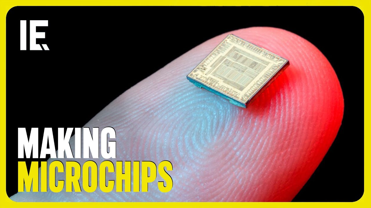
💻 How Are Microchips Made?
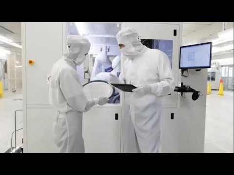
Fabricação de Chips - Como Microchips são feitos? - Infineon (Tradução e dublagem: Matteo Reis)
☝🏻КРИЗИС NVIDIA: мощь Ryzen 9000, SoC Nintendo Switch 2, Intel в Узбекистане
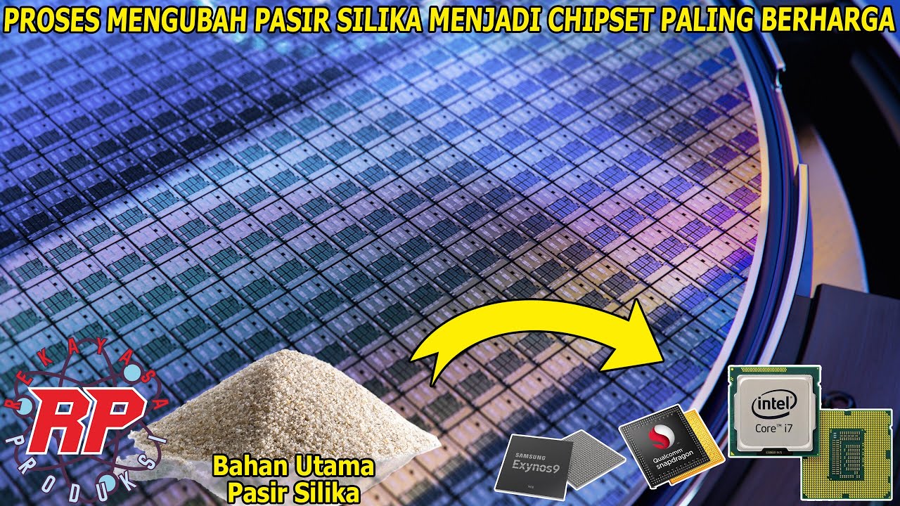
INTIP PROSES PRODUKSI CHIP SEMIKONDUKTOR TERMODERN DARI SILIKON MURNI KE REVOLUSI DIGITAL PROCESSOR
‘Semiconductor Manufacturing Process’ Explained | 'All About Semiconductor' by Samsung Semiconductor

Solar Module Manufacturing
5.0 / 5 (0 votes)
