How do Electron Microscopes Work? 🔬🛠🔬 Taking Pictures of Atoms

Branch Education
25 Sept 202319:54

Summary

TLDRThis script explores the world of electron microscopy, crucial for designing nanoscale transistors and revealing intricate structures like butterfly wing scales. It explains the two main types: SEM for surface imaging and TEM for internal structures, highlighting TEM's ability to resolve individual atoms. The script delves into the physics of electron manipulation, the engineering of magnetic lenses, and the technological advancements that have made such high-resolution imaging possible, with a special thanks to sponsor Thermo Fisher Scientific.

Takeaways

  • 🔬 Electron microscopes revolutionize the way we observe the micro and nanoscopic world, enabling the imaging of structures as small as individual atoms.
  • 🦋 The European Peacock Butterfly's wing showcases the difference between light and electron microscopy, with the latter revealing intricate details invisible to the naked eye or light microscopes.
  • 🔍 There are two main types of electron microscopes: Scanning Electron Microscopes (SEM) for surface imaging and Transmission Electron Microscopes (TEM) for internal structure imaging.
  • 📏 SEMs have a maximum resolution of about 1 nanometer, while TEMs can achieve up to 50 picometers, roughly the size of a hydrogen atom.
  • 🚀 The basic operation of a TEM involves accelerating electrons to nearly 70% the speed of light to create a beam that passes through a specimen, capturing its internal structure.
  • 🧲 Magnetic lenses in TEMs focus and magnify the electron beam, with the objective lens being crucial for defining the final resolution due to its optical aberrations.
  • 🌌 The resolution of electron microscopes is limited not by the electron beam itself but by the aberrations introduced by the magnetic lenses used for focusing.
  • 🔋 A vacuum environment is essential for electron microscopy to prevent scattering of the electron beam by air molecules, which would degrade image quality.
  • 🔬 Thermo Fisher Scientific, the sponsor of the video, provides a 3D model and insight into the complex technology of electron microscopes, emphasizing their role in scientific research and development.
  • 🌐 The STEM (Scanning Transmission Electron Microscope) is a variation of TEM that combines features of both SEM and TEM for enhanced imaging and elemental analysis capabilities.
  • 💡 Electron microscopes are vital tools in advancing scientific knowledge and technology, with applications ranging from material science to nanotechnology.

Q & A

  • What role does the electron microscope play in modern science and technology?

    -The electron microscope allows scientists and engineers to see and analyze structures at the nanoscale, far beyond the capabilities of light microscopes. It has been instrumental in advancing fields like semiconductor technology, materials science, and biology by providing detailed images of materials at the atomic level.

  • How does the Scanning Electron Microscope (SEM) differ from the Transmission Electron Microscope (TEM)?

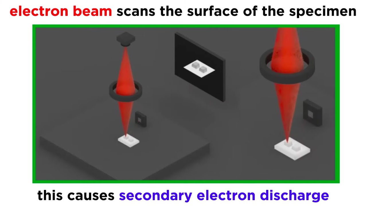
    -The SEM creates images by scanning a focused electron beam across the surface of a specimen, producing detailed surface images. In contrast, the TEM transmits electrons through a thin specimen to capture internal structural details. SEM is better for surface topology, while TEM is used for internal analysis.

  • Why is light microscopy limited in its ability to resolve nanoscopic features?

    -Light microscopy is limited by the wavelength of visible light, which is around 540 nanometers. This wavelength is too large to resolve features smaller than about 300 nanometers, leading to blurred images when attempting to observe nanoscopic structures.

  • How does accelerating electrons to 70% of the speed of light enhance the capabilities of an electron microscope?

    -Accelerating electrons to such high speeds reduces their wavelength to around 2.5 picometers, allowing the microscope to achieve much higher resolution than light microscopes. This enables the visualization of features at the atomic level, which is essential for detailed nanoscopic analysis.

  • What are the main components of a Transmission Electron Microscope (TEM)?

    -A TEM consists of a field emission source to generate electrons, a series of magnetic lenses (condenser, objective, and projector lenses) to focus and magnify the electron beam, and a detector or camera system to capture the final image. The entire system operates in a vacuum to prevent electron scattering.

  • What is the significance of the objective lens in a TEM?

    -The objective lens is considered the heart of the TEM, as it is responsible for the initial magnification and resolution of the image. It determines the final resolution by minimizing optical aberrations, which are critical for achieving clear and detailed images at the atomic scale.

  • Why is a vacuum necessary in the operation of an electron microscope?

    -A vacuum is essential to remove atmospheric molecules that could scatter the high-speed electrons, causing them to deviate from their path and blur the image. The vacuum ensures that the electron beam remains focused and accurate, which is crucial for producing high-resolution images.

  • What are optical aberrations, and how do they affect the resolution of a TEM?

    -Optical aberrations are distortions introduced by the lenses in the TEM, which can blur and reduce the resolution of the image. Despite the potential for incredibly high resolution, aberrations limit the microscope's ability to clearly resolve the smallest features, making it a critical area of focus in microscope design.

  • How does the Scanning Transmission Electron Microscope (STEM) combine features of both TEM and SEM?

    -The STEM operates similarly to a TEM but scans a focused electron beam across the specimen like an SEM. This approach allows it to create images with different contrast mechanisms and perform elemental analysis, making it versatile for detailed structural and compositional studies.

  • What advancements in electron microscopy have been made possible by companies like Thermo Fisher Scientific?

    -Companies like Thermo Fisher Scientific have developed advanced electron microscopes with higher resolution, better imaging capabilities, and more precise control over electron beams. These advancements have enabled breakthroughs in nanotechnology, materials science, and biological research by allowing scientists to observe and analyze structures at the atomic level.

Outlines

00:00

🔬 The Fascinating World of Electron Microscopy

This paragraph introduces the concept of electron microscopy and its significance in understanding the microscopic world. It uses the example of a European Peacock Butterfly’s wing to illustrate how electron microscopes can reveal details invisible to light microscopes, like the intricate texture of scales. The paragraph highlights the importance of electron microscopes in advancing technology, especially in the development of smaller transistors by imaging at the atomic level. It also introduces the two main types of electron microscopes: Scanning Electron Microscopes (SEM) for surface imaging and Transmission Electron Microscopes (TEM) for viewing internal structures.

05:05

🧬 The Limits of Visible Light and the Power of Electrons

This section delves into the limitations of visible light in microscopy, explaining why light microscopes cannot resolve features smaller than 300 nanometers due to the diffraction of light waves. It contrasts this with electron microscopes, which use electrons with much shorter wavelengths, allowing them to achieve resolutions down to 50 picometers, enough to see individual atoms. The paragraph emphasizes the superior resolving power of electron microscopes, crucial for studying nanoscale structures that light microscopes cannot reveal.

10:08

⚛️ How Transmission Electron Microscopes (TEM) Work

This paragraph details the working principle of a Transmission Electron Microscope (TEM). It explains how TEMs generate a beam of electrons accelerated to 70% of the speed of light, which then passes through a specimen, scattering based on its density and composition. The scattered electrons create an imprinted image, which is magnified by a series of magnetic lenses. The process of magnification involves both objective and projector lenses, with the final image captured by a high-resolution camera. The paragraph also touches on the necessity of using electrons instead of light to achieve the high magnifications required for atomic-level imaging.

15:09

🔍 The Complex Engineering Behind TEMs

This section explores the intricate engineering involved in TEMs, starting with the field emission source that generates free electrons. It describes the process of accelerating these electrons and the use of magnetic lenses to focus them onto the specimen. The paragraph also discusses the challenges of controlling electron beams, including the introduction of optical aberrations that limit resolution. The physics behind magnetic lenses and the Lorentz force is explained, demonstrating how magnetic fields focus the electrons to create magnified images. The paragraph concludes by highlighting the additional systems in a TEM, such as phosphorescent screens, CMOS cameras, and various detectors, all contributing to the microscope's functionality.

Mindmap

Keywords

💡Electron Microscope

An electron microscope is an instrument that uses a beam of electrons to create an image of the specimen. It is capable of much higher magnifications than light microscopes, allowing scientists to see structures at the nanometer and even atomic scale. The video emphasizes how electron microscopes have revolutionized our understanding of the microscopic world by enabling the visualization of features far smaller than what is possible with visible light.

💡Scanning Electron Microscope (SEM)

A Scanning Electron Microscope (SEM) is a type of electron microscope that produces images by scanning a focused electron beam across the surface of a specimen. SEMs are primarily used to examine surface structures, with a resolution down to around 1 nanometer. The video highlights SEM's capability to reveal detailed surface topology, such as the intricate textures of a butterfly's wing or the bristles of a used toothbrush.

💡Transmission Electron Microscope (TEM)

A Transmission Electron Microscope (TEM) is another type of electron microscope that transmits electrons through a specimen to form an image. TEMs are used to view internal structures of materials, much like an X-ray shows bones inside the body. The video discusses how TEMs are essential in fields like materials science and biology, with the ability to resolve features down to 50 picometers, such as the atomic structure of a transistor or the internal makeup of cells.

💡Resolution

Resolution in microscopy refers to the smallest distance between two points that can still be distinguished as separate entities. In the context of the video, resolution is critical as it determines how much detail can be seen in the image. The video explains that the resolution of electron microscopes, such as SEMs and TEMs, far surpasses that of light microscopes, allowing for visualization of features at the nanometer and even atomic scales.

💡Nanometer

A nanometer is a unit of length in the metric system, equal to one billionth of a meter (10^-9 meters). In the video, nanometers are used as a scale for measuring incredibly small distances, such as the resolution limits of electron microscopes. For example, SEMs can resolve features as small as 1 nanometer, while TEMs can reach resolutions as fine as 50 picometers.

💡Magnification

Magnification is the process of enlarging the appearance of an object through an optical system. The video contrasts the magnification limits of light microscopes (up to 2000 times) with the vastly superior magnification capabilities of electron microscopes, which can magnify up to 2 million times. This allows electron microscopes to reveal structures at the atomic level that are invisible to light microscopes.

💡Electrons

Electrons are subatomic particles with a negative charge that play a central role in the operation of electron microscopes. The video explains how electron microscopes use beams of accelerated electrons to achieve high-resolution images, as electrons have much shorter wavelengths than visible light, allowing for greater magnification and resolution.

💡Field Emission Source

A Field Emission Source is a device used in electron microscopes to generate free electrons. The video describes how this source operates by using a sharp tungsten needle and a strong electric field to pull electrons away from the tungsten. These electrons are then accelerated to high speeds for imaging, forming the basis of the electron beam used in both SEMs and TEMs.

💡Magnetic Lenses

Magnetic lenses are components in electron microscopes that focus and control the electron beam. The video discusses how these lenses, which are made up of coils of copper wire generating a magnetic field, focus the electron beam onto the specimen and then magnify the transmitted or scattered electrons to form an image. The quality and precision of these lenses are crucial for achieving high resolution in electron microscopy.

💡Aberrations

Aberrations in microscopy refer to distortions in the image caused by imperfections in the optical system, such as lenses. The video mentions spherical and chromatic aberrations, which can limit the resolution of even the most powerful electron microscopes. These aberrations add blurriness to the image, and much of the engineering behind electron microscopes is aimed at minimizing these effects to achieve clear, high-resolution images.

Highlights

Scientists and engineers use electron microscopes to develop transistors as small as the width of a DNA strand.

Electron microscopes allow us to capture images of individual atoms, revolutionizing our understanding of the micro and nanoscopic world.

There are two main types of electron microscopes: Scanning Electron Microscope (SEM) for surface images and Transmission Electron Microscope (TEM) for internal structures.

SEM can reveal incredible details like the texture of butterfly wings or bacteria on human cells, with a maximum resolution of around 1 nanometer.

TEM can capture images of structures inside materials with a resolution of up to 50 picometers, roughly the size of a hydrogen atom.

The TEM operates by accelerating electrons to 70% of the speed of light and transmitting them through a specimen, imprinting an image on the electron beam.

The magnification process in TEM involves magnetic lenses that focus and magnify the image up to 2 million times.

TEM is crucial for developing cutting-edge technology, allowing scientists to see inside materials at an atomic level.

Visible light has limitations in magnification, which electron microscopes overcome by using electrons with wavelengths 200,000 times smaller than visible light.

Magnetic lenses in electron microscopes focus the electron beam, acting like convex lenses but using magnetic fields to control electron trajectories.

Optical aberrations in magnetic lenses limit the resolution of electron microscopes, making reducing these aberrations a key area of research.

The Scanning Transmission Electron Microscope (STEM) combines elements of both TEM and SEM, allowing for elemental analysis and contrast imaging.

Thermo Fisher Scientific, a leader in laboratory equipment, played a significant role in the development and understanding of these microscopes.

The electron microscope's technology is supported by extensive engineering, including vacuum systems, magnetic lenses, and sophisticated imaging detectors.

Electron microscopes are essential tools in scientific research, enabling discoveries in fields like nanotechnology, biology, and material science.

Transcripts

play00:00

Have you ever wondered how scientists and engineers design transistors that are around

play00:05

the width of a strand of DNA?

play00:08

How do we even take pictures of such nanoscopic transistors?

play00:12

Well, that’s the role of the electron microscope which has literally changed the way humanity

play00:18

sees the micro and nanoscopic world.

play00:21

Don’t believe us?

play00:22

Take this European Peacock Butterfly for example.

play00:26

When we zoom in on its wing using a light microscope, we see that it’s composed of

play00:31

tiny overlapping scales.

play00:33

But, when we zoom in using an electron microscope, we can clearly see the shape of each scale,

play00:40

and zooming in further, we see how the scales have a truly incredible texture entirely foreign

play00:46

to anything that humans manufacture.

play00:49

Although this wing may not be directly related to the technology you’re familiar with,

play00:54

scientists and engineers have been using electron microscopes for the past 60 years to develop

play01:00

smaller and smaller transistors, and with today’s technology this microscope can zoom

play01:06

in millions of times to where it’s able to capture images of individual atoms.

play01:13

There are two main types of electron microscopes.

play01:16

The Scanning Electron Microscope or SEM is used to see surface images like this butterfly

play01:23

wing, or the bristles of a used toothbrush.

play01:27

See, here are cells from your body, and all around here in yellow is bacteria.

play01:33

It’s gross, but let’s move on.

play01:37

Scanning Electron Microscopes have a maximum resolution of around 1 nanometer.

play01:42

Meaning the spacing between two adjacent features or dots of resolvable data in an image is

play01:49

1 nanometer.

play01:50

The other type is the Transmission Electron Microscope or TEM which is used to take images

play01:56

of structures that are inside materials, much like an x-ray machine takes pictures of the

play02:02

bones inside our bodies.

play02:04

For example, TEMs are used to take the pictures of these sections of a transistor.

play02:10

However, in other domains of science TEMs can be used to take images of proteins inside

play02:16

mitochondria, the powerhouse of the cell, or of nanoparticles of pure gold.

play02:24

Transmission Electron Microscopes are typically more complex than SEMs and have a resolution

play02:29

up to 50 picometers, which is roughly the size of a hydrogen atom.

play02:35

One quick note is that this video’s sponsor, Thermo Fisher Scientific, provided us with

play02:41

a basic 3D model of one of their transmission electron microscopes and assisted in our understanding

play02:47

of the complex technology involved.

play02:50

Let’s first focus on the TEMs as they are more commonly used in developing cutting-edge

play02:56

technology, and later we’ll provide an overview of the scanning electron microscope.

play03:02

And note that there’s considerable overlap between the engineering inside them both.

play03:07

The basic idea behind a TEM is that it generates electrons and accelerates them to around 70%

play03:14

the speed of light, thus creating a beam of electrons.

play03:19

Next a series of magnetic lenses focuses the electrons down to a small area and shoots

play03:25

or transmits these electrons through the specimen that we’re looking at.

play03:30

Depending on the different densities and materials inside the specimen, the electrons are scattered

play03:35

as they pass through it, thereby imprinting an image of what’s inside the specimen onto

play03:42

the beam of electrons.

play03:43

The imprinted beam of electrons is then magnified 40 times using an objective lens and further

play03:51

magnified 50,000 times using a set of projector lenses.

play03:57

At this point, the imprinted image is 5 or so centimeters wide and large enough to be

play04:02

captured by a high-resolution camera sensor at the bottom of the microscope.

play04:07

We’ll explore the detailed engineering in a little bit, but for now, you might be wondering

play04:13

why do we have to go through the hassle of manipulating electrons, and why can’t we

play04:18

just use light?

play04:19

Well, visible light is physically limited to magnifications up to around 2000 times,

play04:25

and, if you try to zoom in further the image remains blurred without revealing any more

play04:31

details.

play04:33

On the other hand, electrons can reach meaningful magnifications up to 2 million times.

play04:40

Why then is light physically limited?

play04:42

Well, let’s return to this image of the European peacock butterfly and the scales

play04:47

on its wings.

play04:48

This image was captured with a camera, this image was taken with a light microscope, and

play04:55

these images were captured with an electron microscope.

play04:59

Let’s consider two features from the specimen that are only 100 nanometers apart.

play05:05

Visible light has an average wavelength of 540 nanometers, which is larger than the distance

play05:11

between these two points.

play05:12

Due to the physics of waves, as light hits these two features it’s bent around, thus

play05:18

creating a pair of propagating waves with a diffraction pattern resulting from the interference

play05:24

of the two waves.

play05:26

If the features are substantially closer than the wavelength of visible light, then the

play05:31

diffraction pattern will make the two features appear like a single blurred feature.

play05:36

In short, visible light can’t really resolve features that are less than 300 nanometers

play05:42

apart.

play05:43

However, in this electron microscope, electrons are accelerated to 70% of the speed of light

play05:50

and have a wavelength of 2.5 picometers which is around 200,000 times smaller than visible

play05:57

light’s wavelength.

play05:59

In principle, such an electron microscope could resolve features spaced just 1 picometer

play06:05

apart, but, due to the magnetic lenses’ physical limitations the real resolution is

play06:11

around 50 picometers, which is enough to see individual atoms in a material.

play06:17

Also, if you’re wondering about the scale of micrometers, nanometers, and picometers,

play06:23

here’s a comparison of the size of each unit.

play06:27

Note that there are many more details and facts that were cut from this video’s script

play06:31

and thrown into the creator’s comments which you can find in the English Canadian Subtitles.

play06:38

That said, let’s now dive into the complex science and engineering behind each part of

play06:50

this Transmission Electron Microscope.

play06:53

We’ll begin at the top with a device called a field emission source which generates free

play06:59

electrons.

play07:00

The basic principle is that negatively charged electrons are attracted to positive electric

play07:06

fields.

play07:07

Here we have a tungsten crystal needle, and below is a ring called the extractor.

play07:13

This extraction ring is connected to positive 5 thousand volts, and as a result the negatively

play07:19

charged electrons in the tungsten are pulled towards the extractor.

play07:24

The electric field’s effect on the electrons is amplified by the sharply pointed tungsten

play07:29

crystal, which is only a few nanometers wide, and as a result the electrons are freed from

play07:35

the tungsten.

play07:37

The next step is to accelerate them to 70% the speed of light.

play07:41

To do this we use a series of metal rings which are graduated to be tens of thousands

play07:47

of volts apart from one another.

play07:49

And, just like before, these positively charged rings use electrostatics to attract the negatively

play07:56

charged electrons which are accelerated through the center of the rings.

play08:01

There are two key reasons for the incredible speed of the electron.

play08:06

First is so they can travel through the specimen, whether it be a transistor, protein or a crystal

play08:12

lattice or something else that has been sliced to typically only 100 nanometers in thickness;

play08:18

and second, as mentioned earlier, electrons exhibit wavelike properties, and the faster

play08:24

they are, the shorter the wavelength and the higher the resolution achievable.

play08:29

One important detail is that when the microscope is running and electrons are being accelerated

play08:34

to relativistic speeds, vacuum pumps are used to remove all the atmospheric molecules, thus

play08:41

creating a vacuum, similar to the vacuum of outer space.

play08:45

This is because incredibly fast-moving electrons will scatter in random directions as they

play08:51

collide with air molecules and thus ruin the images of the specimen.

play08:56

Now that we have a beam of electrons, we’ll explore the magnetic lenses of which there

play09:01

are essentially three sets: the condenser, the objective, and the projector.

play09:08

The role of the condenser magnetic lenses is to focus the electrons from the source

play09:14

and project them onto the sample so that they illuminate an area the size of a micrometer

play09:19

to several nanometers depending on the desired magnification.

play09:24

Additionally, the microscope uses apertures, or holes placed in the path of the beam to

play09:31

filter out any electrons that are fanning too far from the center of the column, or

play09:36

optical axis, resulting in electrons more parallel to one another before they hit the

play09:42

specimen.

play09:43

The specimen is placed on a holder which is inserted through an airlock into the vacuum

play09:48

chamber.

play09:49

To see different aspects of the specimen such as the crystal lattices, the holder can move,

play09:55

or translate the specimen in all three directions, X,Y, and Z, and rotate the specimen along

play10:02

the X-axis, and with some holders, also the Y-axis.

play10:07

With this we can get images exactly perpendicular to the features such as these transistors

play10:14

inside.

play10:15

The incredibly small beam then hits the specimen composed of different elements and densities

play10:21

of materials, thus scattering the electrons in different ways thereby imprinting an image

play10:27

on the transmitted electron beam.

play10:30

The next lenses, the objective and a series of four projector lenses, are used to resolve

play10:37

and magnify the miniscule image imprinted into the electron beam up to a width of a

play10:43

few centimeters.

play10:45

This process is separated into two parts.

play10:48

First the objective lens – often considered the heart of the microscope – magnifies

play10:54

the image by 40 times and its optical aberrations define the final resolution.

play11:01

Then the projector lenses magnify the image the rest of the way by 50,000 times.

play11:07

What are optical aberrations and why is 2 million times the typical maximum magnification?

play11:14

Well, let’s look at this image of 962 blurry atoms of gold.

play11:20

With today’s technology, the TEM’s ability to resolve the smallest features is not limited

play11:26

by the electrons in the beam, but rather by the lenses and the aberrations and distortions

play11:32

that they add to the image-imprinted electron beam after it has been magnified.

play11:38

There are a few main types of aberrations such as spherical and chromatic, which we

play11:44

won’t explore further, but the main idea is that perfectly controlling a beam of electrons

play11:50

is far from trivial and the aberrations add blurriness and impede resolution after the

play11:57

magnification.

play11:58

The projector lenses magnify what has already been magnified by the objective lens, including

play12:04

the added aberrations, and this second magnification adds its own aberrations afterwards.

play12:10

Therefore, a considerable amount of science and engineering is dedicated to reducing the

play12:16

aberrations introduced by the objective lens, as that is what ultimately limits the sub-nanometer

play12:23

scale resolution of the microscope.

play12:26

One thing you’re probably wondering is why these magnetic lenses look nothing like microscope

play12:32

or camera lenses and how do magnetic lenses operate on fast moving electrons?

play12:37

Well, inside the lens is a coil of copper wire surrounded by an iron housing.

play12:44

When a current is run through these coils, a magnetic field is produced.

play12:49

This magnetic field is then routed through the iron to the pole pieces where it’s channeled

play12:55

into an optical column.

play12:57

These magnetic fields are then used to change the trajectory of the electron by bending

play13:02

the electrons towards the center, or optical axis, in a shrinking helical direction.

play13:09

The physics at play is the Lorentz Law.

play13:12

To summarize, the force on the electron is equal to its charge, Q, times V or the electron’s

play13:20

velocity vector crossed with B, the magnetic field vector.

play13:25

In short, if the electron were to have a velocity away from the optical axis, it would be forced

play13:32

by the magnetic field down towards the center.

play13:36

However, if the electron were traveling perfectly down the center along the optical axis, it

play13:42

wouldn’t experience any Lorentz force from the magnetic fields and would just continue

play13:47

down the center.

play13:49

As a result, the magnetic lenses act as convex or converging lenses, focusing all the electrons

play13:56

down to a focal point.

play13:58

As the electrons continue their trajectory past the focal point and expand, they produce

play14:04

a magnified image.

play14:06

This magnification depends on the strength of the magnetic fields, the position of the

play14:11

lenses, and the position of the detectors and cameras.

play14:15

Let’s move further down the microscope and explore how we turn electrons into images.

play14:21

There are two separate systems.

play14:23

First, we have a phosphorescent screen which has a special coating that glows when electrons

play14:29

hit it and a camera is used to view the screen.

play14:33

This system is used to align the microscope and provide an overview of the specimen.

play14:38

When you’re ready to capture a high-resolution image, the phosphorescent screen moves out

play14:44

of the way, and the image is captured using the second system with a more sensitive CMOS

play14:49

camera that has a higher resolution and dynamic range.

play14:53

The purpose of having two systems is that the phosphorescent screen and camera is used

play14:59

to ensure that the electron beam and magnetic lenses are set up properly, as an incorrectly

play15:05

focused beam could damage the sensitive CMOS camera.

play15:08

We’ve covered many key parts of the microscope, but there are other pieces of equipment and

play15:14

modules that provide additional features.

play15:17

For example, there are X-Ray detectors, energy filters, phase plates, monochromators, multipole

play15:24

correctors, mechanisms to hold and adjust apertures, water cooling for the magnetic

play15:29

lenses, tons of circuitry to control the magnetic lenses and the field emission source, vacuum

play15:36

pumps, power supplies, and much more.

play15:40

Additionally, the entire microscope sits on air cushions to remove external vibrations.

play15:46

Undoubtedly, this microscope represents an incredible amount of science and engineering,

play15:52

and we’re thankful to this video’s sponsor, Thermo Fisher Scientific, for allowing us

play15:57

to look inside.

play15:59

In addition to electron microscopes, Thermo Fisher also makes a wide range of laboratory

play16:04

equipment such as centrifuges, incubators, x—ray and mass spectrometers, and in fact

play16:12

they make PCR systems that can be used to test for Covid 19.

play16:17

Undeniably, Thermo Fisher products are some of the backbones of scientific research in

play16:22

labs across the world.

play16:24

Thermo Fisher isn’t sponsoring this video because they want you to buy a multi-million-dollar

play16:29

electron microscope, but rather, just like us at Branch Education, they believe that

play16:35

the future of humanity lies in the hands of scientists’ and engineers’ abilities to

play16:40

discover, innovate, and engineer solutions to the problems that face humanity.

play16:46

If you’re pursuing a career in science or engineering, take a look at Thermo Fisher

play16:51

Scientific.

play16:52

You too could work on creating the tools that propel science and engineering forward.

play16:58

Now that we understand the transmission electron microscope, let’s look at the Scanning Electron

play17:05

Microscope or SEM which Thermo Fisher Scientific also manufactures.

play17:10

The main idea is that, instead of illuminating an area of a specimen and imprinting the image

play17:15

all at once, with a SEM we create a focused spot, and scan this spot across the object

play17:23

we’re trying to magnify.

play17:24

These electrons then bounce off, and, in the process, create secondary electrons, back-scattered

play17:31

electrons and X-Rays, which we measure to get details as to the surface topology and

play17:37

chemical composition.

play17:39

For example, this process was used to create these images of the butterfly wing, or of

play17:45

this salt crystal.

play17:47

The issue with SEM is that it only takes images of the surfaces of materials and the resolution

play17:53

is limited by how small we can create the focused spot and by how deep the electrons

play17:59

penetrate into the sample, or the so-called interaction volume.

play18:03

The practical resolution is typically around 1 nanometer.

play18:08

Additionally, a useful variation of the Transmission Electron Microscope that’s worth mentioning

play18:14

is called an STEM, where the S is for scanning.

play18:18

This microscope is similar to the TEM, but like the SEM, we focus the beam into a spot

play18:25

and then use deflection coils to scan the spot through the specimen.

play18:28

The benefit of STEM is that it has a different mechanism for creating image contrast and,

play18:36

when paired with an x-ray detector, is capable of elemental analysis of the sample.

play18:42

More expensive TEMs typically have the optical elements and circuitry to perform both TEM

play18:48

and STEM, and the user can toggle between the two modes.

play18:53

We’re sure you have many questions; feel free to put them in the comments below, and

play18:59

we’ll try to answer them in the top pinned comment.

play19:02

Also, one of the scientists from Thermo Fisher who works on these microscopes and helped

play19:07

us to research and write this script, has written the creator’s comments with loads

play19:12

of additional information, so take a look at them in the English Canadian Subtitles.

play19:18

We believe the future will require a strong emphasis on engineering education and we’re

play19:24

thankful to all our Patreon and YouTube Membership Sponsors for supporting this dream.

play19:29

If you want to support us on YouTube Memberships, or Patreon, you can find the links in the

play19:34

description.

play19:36

This is Branch Education, and we create 3D animations that dive deeply into the technology

play19:42

that drives our modern world.

play19:44

Watch another Branch video by clicking one of these cards or click here to subscribe.

play19:51

Thanks for watching to the end!

Rate This

5.0 / 5 (0 votes)

相关标签
Electron MicroscopyNanotechnologyScientific ResearchMicroscopic ImagingSTEM EducationInnovationTechnologyAtomic ScaleThermo FisherEducational Animation
您是否需要英文摘要?