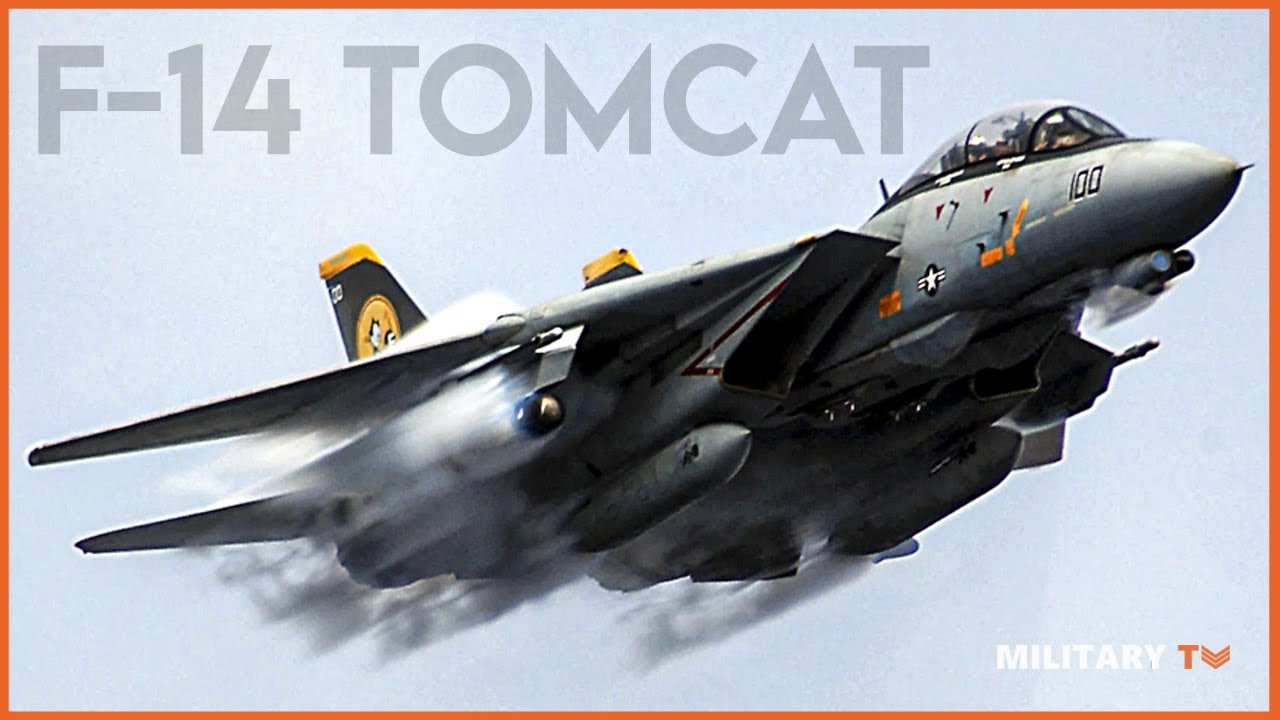
The World's First Microprocessor: F-14 Central Air Data Computer
Summary
TLDRThe MP944 microprocessor was developed in 1970 for the F-14 fighter jet and was far more advanced than the Intel 4004, often considered the first microprocessor. The MP944 utilized parallel processing and pipelining to perform complex calculations for the jet's fly-by-wire system. Though largely forgotten today, analysis of the MP944's innovative architecture suggests home computing could have progressed very differently if knowledge of it had been made public earlier.
Takeaways
- 😲 The MP944 microprocessor was developed in 1970, before the Intel 4004, and was much more advanced
- 🤓 The MP944 consisted of 6 ICs - CPU, ROM, RAM, parallel multiplier, parallel divider, and data steering unit
- 🛫 It was used in the Central Air Data Computer for the F-14 Tomcat fighter jet
- 💪🏼 The MP944 could perform arithmetic on 20-bit numbers at high speed using parallel processing
- 🤔 There is debate over whether the MP944 or Intel 4004 was the first true microprocessor
- 👷♂️ The entire 6000+ bit MP944 program was hand-coded in binary in just 3 months
- 🔬 The MP944 chips were tested using a software simulator and a hardware simulator
- 😎 The MP944 automated control of the F-14's variable wing geometry during flight
- ❌ The MP944 project was kept secret by the US military for over 25 years
- 🪦 Iran maintains the last F-14s still in service, but lacks MP944 chips due to US destruction of stock
Q & A
What was the MP944 microprocessor used for?
-The MP944 was used as the central processing unit for the Central Air Data Computer (CADC) on the US Navy's F-14 Tomcat fighter jet. It provided flight control, instrumentation, and weapons systems functionality.
How did the MP944 compare to other microprocessors of the era?
-The MP944 was far more advanced than other microprocessors of the early 1970s. It had a 20-bit architecture, parallel processing capabilities, and innovative design features that weren't seen in consumer chips until the 1980s.
Why was the MP944 kept classified for over 25 years?
-The MP944 was part of the classified avionics system of the F-14 Tomcat. Revealing its capabilities could have compromised national security. It was only declassified in 1998 after the F-14 was retired from frontline US Navy service.
What made programming the MP944 challenging?
-The MP944 had no compiler, so its roughly 3000 instructions of code had to be written in binary machine code. Also, code had to be simulated before being burned onto physical ROM chips since changes were difficult.
How did the MP944 achieve high performance?
-Through parallel processing units, pipelining, optimized hardware for key operations like multiplication, and innovations like adding numbers as they were transferred between chips.
What was innovative about the MP944's architecture?
-It had separate chips for critical tasks like I/O, steering logic, arithmetic, and control flow. This modular architecture with dedicated hardware units enabled high performance.
How were the MP944 chips tested?
-The team wrote test programs that executed on every transistor to detect failures. They also built a physical simulator from discrete components to functionally validate the chips.
Why did the F-14 Tomcat need such an advanced flight computer?
-The F-14 was designed to be an agile, maneuverable fighter for air combat and ground attack. The MP944 automated complex tasks like sweeping the variable-geometry wings during high-G maneuvers.
What happened to the F-14 Tomcats still flying?
-Some F-14s remain active in the Iranian Air Force, having been sold to Iran before the 1979 revolution. The US destroyed its remaining F-14 fleet in 2006 to prevent spare parts from reaching Iran.
Could the MP944 have changed the course of computing history?
-Possibly, if its design had been made public earlier. The MP944's advanced architecture could have influenced microprocessors for personal computers in the 1970s and 80s.
Outlines
😀 Fading fads and cutting edge tech of the early 1960s - IBM 1401 and PDP-1
The two popular but extremely expensive and bulky computer options in 1961 were the IBM 1401, weighing over a tonne and costing $3.5 million in 2024 dollars, and the lighter but still large and costly PDP-1 at 730kg and over $1 million in 2024 dollars. The high price was due to the discrete transistor technology requiring extensive manual assembly.
😎 F-14 Tomcat - most intimidating fighter jet with swing wings needing computer control
The F-14 Tomcat was designed to replace the F-4 as the US Navy's carrier aircraft, with its variable wing geometry giving it a highly distinctive and intimidating appearance. The position of the swing wings was automatically controlled by the Central Air Data Computer (CADC) to ensure optimal configuration for speed and altitude without pilot input.
😖 Complex supersonic aerodynamics solved in hardware not software
The CADC's microprocessor MP944 differed from the general purpose Apollo Guidance Computer by solving difficult aerodynamic problems via specialized hardware rather than complex software. This included parallel processing units for fast multiplication and division but required programming in binary since there was no compiler.
😮 MP944 - 6 chips forming a complete and bizarre computer
The MP944 consisted of 6 chips - CPU, RAM, ROM, parallel multiplier, parallel divider, and data steering unit which handled I/O. The limited pins required serial communication, slowing transfers but the parallel units enabled simultaneous operations. Multiple units controlled by individual ROMs formed the complete CADC system.
😯 Intel 4004 - remarkable yet highly compromised achievements
Despite its historical significance, the Intel 4004 was extremely limited compared to the MP944, with only a 4-bit bus enabling a max count of 16. Instructions had to be serialized across 8 cycles with no pipelining. However, producing the 4004 cheaply still required multiple innovations.
🤔 Complex definitions - what was the first microprocessor?
There is no consensus on the first microprocessor given ambiguities over required number of chips and functionality. The MP944 appears to predate the 4004 and offered far greater capabilities but relied on 6 chips. The definition focuses on commercial availability rather than purely technical milestones.
😊 Extreme MilSpec design requirements - impressive innovations
Impressively, the MP944 CADC met military specifications, operating from -55C to 125C. Real-time failure detection was implemented by software checks on every transistor. Serial interfaces between limited pins were used to meet size constraints of a 40 square inch board.
🤯 Parallel processing enabled 600 calculations per 1/18 second
Parallel processing units for multiplication and division enabled the CADC to perform the required 600 calculations every 1/18th second. The CPU specialized in limit functions, while addition/subtraction occurred in the data steering unit, maximizing parallelism across the architecture.
😵💫 Programming marathon - simulating hardware before manufacturing
The entire CADC program was coded in 3 months in pure binary since no compiler existed. A hardware simulator using discrete components and a Fortran software simulator were used to validate the 6000+ bit program prior to burning the final ROMs.
🏴☠️ F-14s still flying in Iran - MP944 chips may be only remaining examples
Due to ongoing Iranian operation, destroyed US F-14 stocks may mean Ray Holt's personal MP944 chip collection are the only surviving samples. The classified nature of the project means its historical significance was unknown when wiped.
Mindmap
Keywords
💡Microprocessor
💡MP944
💡Intel 4004
💡CADC
💡Parallel processing
💡Pipelining
💡MilSpec
💡Swing wings
💡Fly-by-wire
💡Classified
Highlights
The MP944 microprocessor was completed in June 1970, over a year before the Intel 4004 was released in November 1971.
The MP944 consisted of 6 ICs - CPU, RAM, ROM, parallel multiplier, parallel divider, and steering logic unit.
The MP944 had a 20-bit architecture and could natively handle integers between -524,288 to 524,288.
The MP944 CPUs specialized ALU was optimized to perform limit functions frequently required for flight calculations.
The MP944 used pipelining and parallelization techniques to maximize performance from its 375 kHz clock speed.
The MP944's parallel multiplier and divider were some of the most complex chips of their time.
The MP944's entire 60000 bit program was written in binary in just 3 months.
The MP944 was much more application-specific compared to more general-purpose consumer microprocessors.
The Intel 4004 was designed primarily for calculators with its simple 4-bit architecture.
The 4004 required instructions to be serialized across 8 clock cycles due to its 4-bit data bus.
The 4004 had only 640 bytes of RAM available compared to the MP944's dedicated RAM chips.
The MP944 was significantly more complex and faster than the 4004.
The F-14 Tomcat was the first aircraft to utilize a microprocessor-based flight computer.
The MP944 enabled advanced functions like automated wing positioning and integrated weapons systems.
Iran operates the last remaining F-14 Tomcats, having kept them operational for over 40 years.
Transcripts
It's late 1961: let's go shopping for a cheap, small computer. The popular choice is this:
this badly green screened IBM 1401. Complete with a punch card reader and printer, it weighs about a
tonne and costs about $3.5 million in 2024 money. If that's a little too much, you could always try
out one of these: a PDP-1. At 730kg and a touch over $1 million 2024 dollars.
There are other options available, but none weight less than a grand piano. And all cost more than a
mansion. That is because every digital computer currently in production comprises of individual,
or discrete, transistors. These must be installed individually into circuit boards,
which are connected into logic units, to form a processor. Collectivley, these draw a lot of
power, create a lot of heat, require a lot of room and require a lot of time to assemble.
Now let's skip forward just 10 years to late 1971. You, a member of the public, can order one of
these for just $450 in 2024 money. This is a fully functional processor on a chip: a microprocessor.
It is several orders of magnitude smaller and cheaper than the mainframes of the early 1960's:
quite an astonishing change in just a decade. As far as almost everyone on Earth is concerned,
this is the first chip-scale processor ever developed.
Now let's skip forward another 27 years to 1998. A paper from 1970 is quietly declassified. It turns
out there was another microprocessor in existance more than a year before the 4004 was released:
it was called the MP944. In fact, it was significantly more advanced than the 4004:
boasting some features that weren't seen in consumer microprocessors until the 1980s.
Why was this pivotal piece of computing history kept secret for more than 25 years? Because the
MP944 was the Air Data Computer for the US Navy's flagship fighter jet: the F-14 Tomcat.
OK, and back to the present day. Every video I ve made in the past has
been about something I d known about for years. This one is a bit different. It was suggested
by a viewer. I ve covered similar topics but I d barely heard of the MP944 until a few months
ago .and reading up on it has been fascinating. It was created by a team of about 25 Engineers
at Garrett AirResearch over the course of 2 years. The designers of the chips themselves
were Steve Geller Ray Holt .someone whos name will crop up repeatedly in this video.
Before we go into the details just a quick couple of points:As with all my videos, this
is arranged into chapters, so feel free to skip ahead if a particular section isn't of interest:
I do tend to go quite in depth on the technical details.We all make mistakes. Unfortunately,
youtube doesn't me to make minor corrections once a video is published. So, if I get anything wrong,
let me know in the comments. However, I will add any known corrections to a pinned comment:
I ask that you check this first before posting. For clarity: MP944 refers to the collection of
chips. These chips were integrated together to form a computer known as
the Central Air Data computer, or CADC. So, the mp944 was the microprocessor,
the cadc was the computer. Let's take a step back and discuss the F-14. I've
stirred up controversy in the past by saying this. 'Most supersonic aircraft are inherantly unstable.
That's the reason most of them look really ugly'. 14 year old me would be EXTREMELY angry if he
heard me saying that. So let me clarify what I meant there. If you are like 98% of my audience,
you are a man. Go and find the nearest woman or child and ask them what is the best looking of
these aircraft. They'll usually pick the one that isn't big scary and pointy. Years ago I helped out
at an airshow, I was showing visitors around the RAF trainer aircraft: one of these. We were parked
right next to a Tornado fighter....and we assumed no one would care about our tiny little propellor
plane. We were wrong: we were totally inundated with kids who wanted to sit in the actual plane,
not the weird looking jet. So that;s what I mean when I say
'ugly'. Fighter aircraft are most certainly not designed to look good. But a side effect
is they tend to look pretty intimidating. And the most intimidating looking fighter ever
built has to be the F-14. Designed to replace the F-4 as the US Navy's main carrier aircraft,
it served until 2006 for the US military. In fact....some are still in service with
the Iranian air force today but that's something we'll come back to later.
Now, I can;t really talk about this jet without mentioning one of the reasons it is famous. It
was in top gun. You know, the film about volleyball. And I'm going to stir up more
controversy here.....I don;t understand why that film was so popular. Is it one of those bad films
that people pretend to like to be funny and I m not getting the joke? I don t know, I'll leave
it there and not mention top gun again.... One of the reasons it is so distinctive is also
the reason it needed a flight computer: variable wing geometry...also known as swing wings.
Every time I try and discuss supersonic aerodynimics I get something wrong so
we're going to keep this really simple. When flying at low speed, for example on approach
to landing, we want as much lift as possible to maintain stable flight. This is when the F-14
would swing the wings forward into what I like to call the 'T-pose'. However, that creates a
high aspect ratio, which creates drag. So, if we want to go fast, we go from a 'T-pose' into what
I call the 'Naruto Run' configuration. Jokes aside, improvements in aerodynamic
computation and design in recent decades have rendered variable wing geometry obsolete. But
these were all the rage in the 1960s and 70s. With the computer enabled, the wing position
was set automatically with no pilot input. This ensured the aircraft was
in the appropriate configuration for the given speed and altitude. Furthermore,
it reduced task loading on the pilot and reduced the chance of the configuration being changed
during the wrong phase of flight. In a previous video, I heavily criticised Virgin Galactic for
not using a flight computer to actuate the rotating wing on spaceshiptwo. In fact, that
was the cause of a fatal accident in 2014. It's nice to know the F-14 was able to autonomously
change it's wing geometry via a computer more than 40 years before spaceshiptwo first flew.
Earlier similar aircraft such as the F-111 were notoriously difficult to control during
the transition from one wing configuration to another. It's not difficult to imagine why:
swinging the wings completely altered the flight characteristics of the aircraft in a
few seconds. And this may be carried out whilst flyting at transonic speeds....where flight
characteristics are already unpredictable. I always imagined the F-14 would require straight
and level flight and a lot of care to transition from one configuration to the other. And I was
completely wrong. There are videos of it sweeping the wings back and forward while inverted,
mid maneuver, in steep banks. Think of an attitude and there is probably a video of an F-14 activley
sweeping its wings back whilst in that attitude somewhere. As most of these videos are from
airshows, the pilot manually overrode the computer to select the wing position. But the movement
itself was still controlled by the computer to ensure stable flight was maintained.
When the wings were swept back, this posed another problem I've discussed previously
on this channel. Those large lifting surfaces moving backwards moved the centre of pressure
backwards. Normally this is a good thing: we want the centre of pressure to remain
behind the Centre of gravity to maintain stable flight. But in this case, it was too far back:
reducing maneuverability....not something you want for an aircraft designed for dogfighting.
So, small surfaces could be extended from the front of the wings. These were known as glove
vanes. Again, it wouldn;t be desirable to extend these at a fixed rate as they would
radically alter the aircrafts handling in a matter of seconds. So, the computer also
controlled the extension and retraction of the glove vanes. Later in the F-14s life,
these tended to be disabled altogether due to their mechanical complexity....but the computer
was always able to control them if needed. The final mechanical output controlled by the CADC
was the maneuvering flaps. The primary control surfaces for rolling were the tailerons and
spoliers, though the latter could only be employed at low speed. However, by partially extending the
flaps, the F-14 was able to enter a tighter roll than would be otherwise possible. If the flaps
were set to maneuvering mode, the CADC actuated them automatically to meet the pilots inputs.
So, physically, the CADC was required to actuate some of the F-14s secondary control surfaces:
namely the variable wings, glove vanes and maneuvering flaps. Not quite a full
fly-by-wire aircraft....but the CADC did act as a fly-by-wire computer for these surfaces.
But it wasn t called the Central Partial Fly by wire computer , so what about the Data in CADC?
Anyone who has flown a light aircraft will be familiar with the mechanical instruments which
are able to convert air pressure and temperature to readings such as airspeed and altitude. At
high airspeeds and altitudes however, this is surprisingly difficult. Due to factors such
as the compressibility of air and changing mach limit with temperature, the formulae to
determine speed and altitude become non linear. So, a simple mechanical indicator is no longer
sufficient. Supersonic aircraft of the 1960s such as the F-4 used complex mechanical computers to
provide flight data to the pilot. The CADC, however, was the first microprocessor based
flight computer to achieve this. Specifically, it provided altitude, temperature and airspeed
to the pilot .and probably some other metrics that I can t find references to.
And this leads us onto the final function of the CADC. It provided necessary data to the weapons
system. The F-14 had a particularly advanced weapons system for the time,
able to track and target multiple airborne targets simultaneously. Six simultaneously
to be specific. Prior to firing air-to-air missiles, the state vector of the missile was
passed to the weapons system. A crucial metric was the angle of attack of the aircraft, as this would
determine the initial attitude corrections necessary for the missile after firing.
The needs of the weapons system also give an insight into the requirement for a 20
bit data length. The required resolution for the altimeter was just 1ft. Smart bombs did
not yet exist, so to line up for a bombing run, the speed and altitude of the aircraft were used
to predict the ballistic trajectory of a bomb, providing the pilot with an optimised time to
release. In fact, the aircraft was flown on altitude hold during a bombing run.
With a service ceiling around 50000ft (which is already a 16 bit number), high altitude runs
could foreseeably take place in rarefied air where the difference in pressure between altitudes was
minimal: hence the need for 20 bit precision. And with that, let's learn about
microprocessors. The term 'microprocessor'
was barely used during the early 1970s. It was largely retroactivley applied to all the
devices we'll discuss. Ironically, it isn't a common term today either what was called a
'microprocessor' in the past is now referred to as a CPU. More specialised hardware such
as GPUs, microcontrollers and FPGAs would also fall under the definition of microprocessor.
So, what IS a microprocesssor? There is no official definition as
such. So let's just go with Wikipedia. That states 'A microprocessor is a computer processor where
the data processing logic and control is included on a single integrated circuit (IC), or a small
number of Ics'. And with that we immediately run into an ambiguity. 'A small number of Ics'.
What exactly is defined as 'a small number'? Does something that can only input operate
on and output 1 bit count as a microprocessor? Do the logic elements all have to be on one chip?
The Intel 4004 is most commonly cited as the first Microprocessor, it was part of a 4-chip collection
referred to as the MCS-4. We will be exploring the 4004 in more depth later. However, the Intel
4004's claim is far from solid. In fact, Intel themselves refer to it as the first 'commercially
available' microprocessor. Let's compare it with the MP944. And, I'll warn you, we are going
to be seriously splitting some hairs here. Ok so which came first? There is no contest here.
The MP944 chipset was completed in June 1970. The first 4004 was produced in January 1971, with the
first sales to the public in November 1971. Now let's look at capability.....briefly. We'll
do a whole chapter on capability later. The MP944 could perform logic and arithmetic operations
on 20 bit numbers. The first bit was used to denote a negative or a positive number. This
means the processor could nativley handle integers between negative and positive 524288. It is always
possible to handle numbers outside of this range, but that requires significantly more compute time
as we have to deal with overflow arithmetic and store/process the intermediate results.
The 4004.....it could handle just 4 bits. Meaning it could nativley handle numbers between 0 and
15. It's really not much. Now, this was enough to build a calculator (we assign a 4 bit value
to every integer in a number)....but even that required significantly more code than
an 8 bit or higher processor. You couldn't , for example, build a practical desktop computer
with a 4 bit processor. This is the first of many controversial statements during this video....but
I reckon there's even a debate to be had as to whether a 4 bit system is complex enough to even
be called a microprocessor (for the record, I think it still counts but it s not really
the same thing as something like a 6502). Ok, now the big one....the number of Ics. The
biggest common strike against the MP944's claim to first microprocessor is the fact it consists
of 6 distinct Ics. Of course....there is a LOT of nuance to this. Two of these are
the ROM and the RAM, so we can discard those as being part of the actual microprocessor (or can
we?...we'll come back to that). The next two Ics are essentially specialised coprocessors:
the parallel divide unit and the parallel multiply unit. These do exactly one thing:
they take two numbers and either multiply or divide them. Now....perhaps we require the
presence of these two chips for the system as a whole to work? No. We don't. This often overlooked
sentance from Holt's 1971 paper clarified 'each unit was designed to operate as a seperate entity
and could be used without the need of any of the other units'. This is really interesting:
in theory any chip from the system as a whole is able to operate by itself....so how many do
we need to form a full-blown microprocessor? The final 2 chips are the steering logic unit
and the CPU. Now in theory you could feed in a sequence of pulses into the appropriate pins of
the CPU to provide it with data and instructions. And you;d receive outputs. But in reality, we need
something manage our various inputs and fed them into the CPU.....and that is the SLU. For now,
we can think of this as an I/O interface between the outside world and the CPU.
It's not really part of the CPU.....it just translates inputs to a form the CPU can use.
So the CPU can in theory operate by itself (or at the very least with an IO chip?). Is
that an unambiguous case of a microprocessor on a single IC?
Unfortunately no. The CPU can perform various logic functions....but it
can't add or subtract. Wait, really? The MP944 did addition and subtraction
on the SLU chips. This actually provided a major benefit as we'll see later. But that
means a minimum of 2 Ics were required. Well...not quite. The CPU COULD perform a
variety of logic functions, and it could perform conditional branching. I'm almost
certain that made it Turing complete....so while it couldn;t add numbers directly,
it could do so indirectly. Making it a viable, yet highly impractical single chip microprocessor.
EXCEPT. The CPU missed something else. It didn;t contain a program counter. This is a register
found in all standard CPUs which keeps track of our current memory location (also knows as
our current place in the program). The program counter for the MP944 was in...the ROM!? So,
while it would probably be theoretically possible to use the CPU chip by itself to perform logic and
arithmetic. To actually run a program and do something useful, we'd need a ROM chip,
an SLU chip and a CPU chip. OK, so for the absolute purists
who insist a microprocessor must consist of a single IC, the MP944 loses to the 4004 right?
Nope....turns out the 4004 couldn;t operate as a single chip either!
As with the MP944's CPU, the 4004 needed a seperate I/O chip to function. In order to get
the logic functionality onto a single silicon die, the 4004 required extensive simplification. One of
the simplified elements was the data decoding: it was not possible to hookup the necessary 12
address pins and 8 instruction pins. So, a shift register chip was necessary in order to transfer
data in and out of the CPU... similar but less advanced than the SLU used in the MP944.
That got complicated quickly. So I'd better throw a final spanner in the works. There
is another entirely seperate contender. The four phase CPU is almost impossible to find
meaningful information on but several hundred were sold in the early 1970s. In terms of complexity,
it sat somewhere between the 4004 and the MP944. Unlike the former 2, the logic functions of the
CPU itself were split between 3 chips. HOWEVER, it was claimed one of these could function in
isolation as a dedicated 8 bit CPU. There is much controversy here, including a court case,
and allegations of deception. If we drop the strict requirement
that a microprocessor must be on a single chip and include the MP944, it feels like
we need to include the 4 phase as well....even though it is 'more' split up than the MP944.
However, it;s probably easier to disqualify it from the title of 'first' based on date. The
four phase system was unambiguously completed in October 1970, when the first sales were made. The
first unambiguous date for the MP944 was June 1970 when it was accepted by the Navy. Of course there
is plenty ambiguity regarding earlier iterations of both designs. The 4 phase system looks
fascinating but there is so little info available on it, it d require an entirely separate video.
So what was the first microprocessor? I don't think it matters. The definition is arbitrary,
ambiguous and outdated. Personally, if you forced me to take a side, I would refer to
the MP944 as a microprocessor.....and probably the first one at that.... You may disagree and
that's fine. But the one thing we can probably all agree on is that the MP944
was incredibly advanced for it's time. Let's find out exactly how advanced it was.
Carrying out any technical contract for the US Military carries a blessing in the
form of practically unlimited potential for funding. It also carries the curse
of stringent requirements. And there were many requirements for the CADC project.
The first was the requirement to operate at MilSpec temperatures. -55C to 125C
specifically. Now, that s not entirely outside the realms of possibility for consumer based
hardware today. But imagine building the world s first microprocessor, only to integrate it into
a computer that was capable of running in a sauna. It s pretty impressive!
Another requirement which had the potential to shelve the whole project was failure analysis.
Every engineer learns about time-based failure prediction. Components tend to fail after a mean
amount of time in use (otherwise known as the mean time between failure). And depending on
how they are used, we can get a good idea on how failures are distributed around this mean.
If one component fails, we can often predict how long it will be before associated parts fail.
It is not difficult to imagine the Military putting a huge focus on these failure metrics.
Weapons systems cost a LOT of money in both capital and maintenance. And they perform life
(and death) critical functions. So, I can only imagine the mounting horror felt by the US Navy
s representative late into the design project when the CADC team sat him down and explained
failure metrics didn t exist for the computer. It was a brand new system with no operational
history and nothing analogous to compare it to. Fortunately, an excellent workaround was devised.
Rather than predicting failure based on past data, with something like a microprocessor,
it is possible to diagnose failure in realtime. After all, a microprocessor and it s associated
memory is really just a collection of transistors. So, by writing programs that execute instructions
that use every transistor at some point and then comparing the output with the expected output,
a single transistor failure could be detected. Through some clever coding,
Ray was able to devise self-diagnostic programs that tested every transistor on 4 of the 6 chips
(including the ROM and RAM by the way). The parallel multiplier and divider chips
were checked for 98% of failure cases, with the remaining 2% being non critical for flight. These
self diagnostic checks were carried out as part of the main program loop. If a failure occurred,
a second completely redundant computer was automatically activated and the pilot
notified by a light in the cockpit. To perform all of the above, the CADC was
required to perform about 600 calculations every 1/18th of a second. And when I say calculations,
I don t mean integer operations, I mean full calculations. The most common calculation was
a 6th order polynomial: like this. However, to obtain a solution, the formula was
rearranged into this form. That required a lot of multiplications, and multiplication takes a while
on a conventional CPU. The MP944 had a clock speed of 375kHZ, so this would give an average
of only 35 instructions per calculation (if we assume one instruction per clock cycle which,
as we ll see, is a very weak assumption). With such a low clock speed, it would be flat out
impossible for a conventional CPU of the day to perform so many calculations so quickly. So now,
we ll take a dive into the architecture of the MP944 which completely set it apart from
anything else that existed at the time. We've already seen the 6 different Ics that make
up the MP944. Let's walk through what each did in detail and how they were integrated
to form a working computer. Ray's paper actually discusses a number of potential configurations,
but we'll look at the one configuration they were used in: for the F-14s CADC.
In essence, the job of the CADC was to take digital inputs from a number of sensors and
turn those into useable outputs. Of course, to process these inputs, a series of instructions
were required: in other words a program. The MP944 microprocessor was a modified Harvard
architecture, with the program and variables residing in seperate memory. The program was
in the ROM, which was the first of the 6 Ics. In the CADC, multiple ROM chips were used to
store the entire program. Overall control was provided by the system executive ROM,
with lesser ROM units supplying instructions to individual compute units. As mentioned,
the program counter was housed in the ROM. This is unusual but was a deliberate choice to reduce
the number of traces on the board since non of the compute units needed to communicate the
program location to the ROM. Therefore this made best used of the available space. I imagine this
would have also made the system more difficult to program but as we ll come back to, that wasn t
really a problem since it needed to be programmed once and once only for its intended purpose.
Outputs consisted of both direct digital signals, and values written to the second of the ICS:
the RAM. As with any conventional computer, the RAM contents could be read as variables
for subsequent program instructions, or they could be output as and when necessary.
So how did the computer get from ROM instructions and digital inputs to stored results in RAM,
and digital outputs? I'm going to work backwards. As we'd expect, there was a CPU:
in this case it was known as the 'Special logic function' or SLF....though I'm just going to refer
to it as the CPU for ease of understanding. Now, I can;t show the exact architecture
for the CPU as it has never been publically disclosed. But here is what we know about it.
Like any CPU, it consisted of a number of registers and an arithmetic logic unit,
or ALU. Values were stored in the registers and basic arithmetic was performed on these
values using the ALU, to give an output. And, as with most early CPU,s the ALU was
capable of basic logical operations. However, this chip differed from a
conventional CPU in several aspects: First of all, it was specialised for
one operation: the limit function. This is a basic operation: shown on screen here it simply
clamps a given input between upper and lower bounding values. This function was requires
so frequently in the flight calculations, that the IC was optimised to perform it. One register
was designated for each of the bounding values, with a third being used for the input. When the
limit operation was performed, the correct register was chosen as the output. I'm not
exactly sure how other logical operations were performed: I imagine the two inputs were stored
in two of the registers, with the third used as an accumulator which is a special register to which
the ALU can write and read from directly. The second unconventional design choice was
the number of pins. Typically, values are passed in and out of a CPU in parallel. In this context,
that means one pin per input and output bit. Remember, the MP944 had a 20 bit architecture,
so when I discuss 'values', I am referring to 20 bit numbers. That would require 20 pins for
the input and 20 for the output. Of course, some additional pins would also be needed for power,
clock, synchronisation, reset and testing. This wasn;t really feasible however. One of
the design constraints from the Navy was for the system to fit on a 40 square inch pcb:
that's just 15x15 cm. Bear in mind, the Apollo guidance computer first flew just 4 years before
the CADC was complete and was considered an absolute miracle of miniaturisation:
it weighed 30kg and was 60x30x15cm. So, the CADC team designed the entire
system to operate serially. Inputs and outputs formed a sequence, broadcast via single pins. The
lower pin count, however, came with the penalty of longer transfer times between compute and memory,
as each 20 bit word now required 20 clock cycles to move from one place to another. It is also
a complete headache to understand...and must have been a nightmare to program.
To generate the serial inputs for the SLU, a dedicated I/O chip was necessary. This
was the Data Steering Unit. Recall the I/O chip necessary to use the intel 4004....this
was SO much more than that. It accepted inputs from either digital sensors, or from the RAM or
ROM and 'steered' these inputs to where they were needed. If i understand correctly, each
SLU accepted up to 13 serial inputs, and could provide serial data to 3 outputs. Through the
use of appropriate commands, the necessary inputs could be sent to the CPU. However, as mentioned,
this chip also had the capability to add and subtract. Data wasn't just steered from input to
output: two inputs could be added or subtracted as they were being shifted. Performing the operation
during the data transfer allows for fast addition: in fact due to some clever design, the SLU could
actually add 3 numbers in the time it took to transfer them from input to output. You can
see here how data was serially shifted through the unit and steered to the required output. Though,
bear in mind I'm showing only 8 bit numbers and 5 inputs: in reality 20 bit numbers were steered
from 13 inputs. In the case of the CADC, each Data Steering Unit only made use of a single output but
other configurations were possible....including using the output from one Steering unit as an
input to another Steering unit. A quick side note: if you can add,
you can also subtract. It is done by converting the binary representation of a number to its 2 s
compliment. The MP944 generally operated on 2s complements but we re not going to
go into any further detail on that here. So what we have here is a complete module.
Able to read instructions and data, steer necessary data to a CPU, and use that CPU
to perform calculations, outputting the results to RAM or directly. But we're not done yet.
What really set the MP944 apart from other early microprocessors were the parallel units:
today we'd refer to these as coprocessors. There were two: the Parallel Multiplier Unit and the
Parallel Divider Unit. Let's focus on the Parallel Multiplier as I think that
one is easier to understand. Functions such as the sixth-order
polynomial I mentioned earlier require a LOT of multiplication, and fast. Early CPUs were
pretty terrible at multiplication....because they couldn;t do it. Well, not directly anyway.
When it comes to multiplication, the only useful arithmetic instructions available in
most CPUs from the 1970s were addition and bit shifting. One way of multiplying x by y was to
add x to itself y times. Of course, for a 20 bit number, this would take practically forever.
The more conventional approach was to use long multiplication....just as we teach
to elementary school children. Here, we take x, multiply it by each bit of y and add the partial
products. But hold on, I just said we can;t multiply. Turns out we don;t need to. Since
we are dealing with binary only, the partial products can be defined conditionally. Every
partial product is either x or zero, because we only ever multiply it by 1 or zero.
However, this still takes a long time...especially for a pair of 20 bit numbers.
So the next approach is to use a specialised algorithm for multiplication. In this case
Booth's algorithm. I was going to explain how this works but that'd take me a while,
so I've linked an excellent video instead. I'm showing an implementation on screen now
for a couple of 4 bit numbers. Now, it is possible to implement Booths algorithm on
a simple CPU. However, without specialised hardware it still takes ages to implement.
So, let's make a more specialised ALU that can perform Booths algorithm in hardware:
it takes x and y and automatically executes the algorithm, sending the result to a third
register. In fact, if we're smart, we could send x and y to this second special ALU....and
while we're waiting for the result, we could perform some other simpler operations on our
first ALU. And we could do addition in the SLU at the same time......we don;t need to
let a lengthy multiplication operation lock up our entire process if we run it in parallel.
And that is the fundemental concept that allowed the designers of the CADC to claw
back time lost to serially moving data: parallelisation. In reality,
this second ALU and its associated registers were housed in a seperate dedicated chip:
the Parallel multiplier. In fact, parallelisation wasn;t the only time saving innovation here. That
time taken to shift the result out of the output register? The next input could be shifted in at
the same time. This approach of overlapping one operation with the next is known as pipelining,
and the MP944 was the first microprocessor to do that too. All the chips I ve discussed
so far were capable of simultaneously shifting data in and out in this manner.
And as I alluded to, there was also a parallel divider unit: basically the same as the parallel
multiplier. I must stress, both of these parallel units were particularly complex for the time just
on their own. Incorporating them into a fully working system was really quite spectacular.
And with that, we have the full architecture. Multiple duplicates of some of the chips
were used in the implementation for the CADC, forming distinct compute units, each controlled
by their own ROM and SL and outputting to dedicated RAM. According to the 1971 paper,
this was the configuration used by the CADC. In total there were 1 of each of the CPU,
PDU and PLU chips; 3 Steering units, 3 RAM chips and 19 ROM chips.
In my video about the Apollo Guidance Computer Flyby wire system....to which I have already
made several refrences, we discussed at length how complex softweare engineering was used to tackle
many of the problems. The Apollo Guidance Computer itself was a reasonably general purpose machine.
In many ways, the MP944 was the opposite. Difficult problems tended
to be solved in hardware rather than software. Any computer executes its code as machine code:
strings of digital inputs represented by binary words. In the case of the AGC,
a compiler was written which allowed programs to be written in assembly language which is
more human readable....this was then converted to binary by the compiler for execution. In fact,
the AGC team also created a higher level language for more complex subroutines. And they were able
to simulate more specialised hardware using what were essentially virtual machines.
The special purpose ALUs, parallel processors and other hardware in the MP944 performed these more
specialised tasks without the need for either highlyt complex subroutines...or simulating
more complex hardware in code. The tradeoff was there was no compiler. Due to time constraints,
all coding was performed in just 3 months. This isn;t necessarily as bad as it sounds:
remember the CADC in which the MP944 was used was application specific: it was designed to do
one thing and one thing only. On the other hand....the team
decided they didn;t have the time to write a compiler....the entire program was written,
not in assembly....but in binary. The final program was over 60000 bits in length, or about
3000 instructions. As was the case with the AGC, it was not possible to continuously develop and
test code snippets on the actual hardware: the ROMs to which the code would be written
required at least several weeks to manufacture. So, it was all or nothing: the entire codebase
was to be burned to the ROM and run in one go. Coding up the ROMS had the additional complexity
of there not being a single monolithic program. Looking at the system architecture, each data
steering unit to compute unit combination required its own set of instructions. So, an
overall program control rom, or program executive was necessary to orchestrate all of the individual
modules (and when I say module , I am referring to both software and hardware). So, individual ROM
chips required their own standalone code. Of course, coding this all in one go is
infeasible: no one can write 3000 instructions correctly without a single mistake. So a means
of simulating the hardware to test out code before final manufacture was required.
Ray s brother, Bill, was actually pulled into the project to solve this. He created a simulator for
the MP944 in Fortran. I ve not been able to figure out exactly what this simulator looked
like but I presume it ran on an IBM mainframe, or something similar. Crucially, it emulated
every transistor in the MP944 chips, and so allowed Ray and the team to test subroutines
without having to create dedicated ROM chips. The second solution was the creation of a physical
simulator. Using discrete components, a mock up of the MP944 was built to function test the hardware
itself. Of course due to the larger scale, it would have run much slower than the chips,
but it was sufficient to prove functionality before the actual chips were manufactured.
Programming took 3 months, with the code being delivered to the manufacturers on punched paper
tape. Floppy drives didn t exist yet so this was the only practical means of doing so. When
the manufactured ROM chips were received a few weeks later, they worked almost flawlessly. A
single bit (out of a total of more than 60000) was incorrect requiring re-manufacture but honestly,
that s about as good a result as anyone can ask for. The corrected ROMS were delivered a few
weeks later, and the completed project handed over to the Navy for evaluation in June 1970.
We ve spoke extensively about what the MP944 chipset could do. Unfortunately,
I can t get my hands on an F-14. So instead let s take a look at the Intel 4004 for comparison:
we'll see it was severly lacking in functionality alongside the MP944. That said, I want to make
clear that the 4004 was still a remarkable achievement for the time: mass producing and
selling it at an affordable price required a number of technological breakthroughs. It also
required some significant compromises. I have one here. In order to use it,
I ve built a retroshield, which is an open source board available here . It allows an
Arduino to simulate the RAM, ROM and IO chip. So, in theory, I can write a program in 4004
assembly and upload it to the Arduino to be run on the 4004. Unfortunately, the documentation
and code for the 4004 retroshield is a bit lacking or incomplete .so I ll just show it
running here. If anyone wants a more detailed video on the 4004 in the future let me know in
the comments but it ll take me a while. The first major compromise was, of course,
the 4 bit data and address bus. As I ve already mentioned, the 4004 could only count to 16. This
does mean it was able to handle a single digit per instruction which leads us onto
it s primary use case. A calculator. The 4004 was specifically designed to be the CPU for the
Busicom 141-PF calculator. It s really not very exciting is it? In fact, the retroshield repo
includes code to emulate the calculator but it doesn t seem to work for me. The 4004 did
see a few other uses, including most notably in pinball machines .but it was too simple a CPU to
see anything requiring anything beyond this. That 4 bit bus simplified the chip design but
complicated programming. 4004 instructions were at minimum 8 bits in length. And the chip could
address 12 bits of memory. So, how do we get these instructions and addressed in and out of
4 bit busses? The answer is to serialise them. Unlike most microprocessors, where instructions
are fed in in a single clock cycle, the 4004 required them to be broken up. Here s how:
The 4004 requires 2 independent clock signals, with a max clock speed of 740 kHz. They must
be provided in the pattern shown here. The chip will response with a sync pulse every
8 cycles .as shown. This pulse denotes the start of a full execution cycle. The required
memory address to read from or write to must be split into 3 4 bit words and provided during
the first 3 clock cycles. Then the instruction to execute must be provided during the next 2.
The final 3 cycles of the execution cycle are used to actually execute the instruction.
Of course, the shift register chip would handle much of the splitting up and
passing of instructions to the CPU. Although the clock speed was 740KHz,
the need for 8 cycles to actually execute anything limited the CPU to 92600 instructions
per second as there was no capability for pipelining or parallel processing.
We should of course note that the MP944 also accepted and output data
in serial but we ve already discussed the extensive design decisions that were
made to negate the time penalty from doing so. A real plus for the 4004 is the registers. It has
16 internal 4 bit registers. Honestly, that s probably enough to do useful things without the
need for a RAM chip at all. If I put my mind to it, I could probably get this running tic tac toe
without any ram .but that s for another time. But, where registers are abundant, a stack
is not. There is technically a stack in the 4004, but it is just 3 addresses deep. So you
couldn;t really use this chip for any recursive operations or nested branching commands.
I also noted whilst playing around with the 4004, it doesn t really feel like a microprocessor. It
is more akin to programming a microcontroller (and yes, I did verbally mix up the 2 in my
previous video). This is due to the modified Harvard architecture. You have to write your
program entirely. Save it to ROM and then execute it. You can t run code from RAM (in fact there are
only 640 bytes of RAM available). Again, this limitation, if you want to call it that, was
also present on the MP944 because the MP944 was designed to do one thing and one thing only.
Which brings me onto my final point about what is and what isn t a microprocessor. The 4004 and the
MP944 were made to perform specific tasks. Off the shelf, the 4004 is probably more versatile due to
the presence of a compiler and a more general purpose arithmetic logic unit. But the MP944
can perform much more complex operations, much faster and provide results to many more outputs.
Most consumer microprocessors are NOT application specific and can be manipulated to perform a wide
range of tasks. So it would be fair to say the MP944 and 4004 are both microprocessors,
or neither is. Either way, the MP944 was significantly more complex.
The only F-14s remaining in service today are with the Iranian air force. How they got there
is a story for another day. The Iranians have managed to keep them flying through
a combination of ingenuity, determination and, I presume pure spite. In fact, some escorted Putin's
entourage into the country just weeks before i released this video. To prevent spare parts
illegally reaching them, the US destroyed it's remaing F-14 stock following their retirement in
2006. Ray has a complete set of MP944 chips in his personal collection. As far as I can figure out,
these may well be the only remaining examples in existance outside of Iran.
Though this feels like a crime against historical preservation, I suppose no-one involved in their
destruction would have had a clue they were wiping out something of such significance.
Through my adult life, I have been through a belief arc that many viewers can probably
relate to. I used to believe all military spending was abhorrant and should instead be directed to
science, medicine, space exploration etc. Then I grew up and accepted we are simply not there
yet. In recent years, I have come to realise that many of the benefits I tout for funding
the sciences are also delivered by the military: a huge proportion of militarty spending IS directed
at science medicine and space exploration! The internet, GPS, encryption technology....the
list of everyday benefits that originated as military backed research is almost endless. So,
do we spend too much on defence? I don't know. The MP944 is not a good example of all of the
above. It didn't change the world, and was a metaphorical dead branch on humanity's
technological tree. It makes perfect sense that the project was classified. However,
looking back more than 50 years later, it seems almost tragic that home computing
could have taken quite a different course had the architecture been made public.
When I made a video about the invention of Digital Fly By Wire, I believed there may
have been only one computer on earth at the time capable of performing the job:
The Apollo Guidance computer. After producing this video, I now know there were two........I wonder
whether there were any more. Thanks for watching.
浏览更多相关视频
The World’s Most Advanced Fighter Jet | F-35 Lightning
8085 Architecture | Learn Intel 8085 Microprocessor Architecture Step - By - Step
Introduction to 8085 Microprocessor (μP)
1 4 Evolution Du Microprocesseur
Introduction to Microprocessors | Skill-Lync
Architecture of 8085 Microprocessor: Data Flow and Working Explained | 8085
5.0 / 5 (0 votes)