Transistors Explained - How transistors work
Summary
TLDRThis video script delves into the intricate workings of transistors, a pivotal invention in electronics. It distinguishes between bipolar and field effect transistors, focusing on the bipolar type, and explains their dual role as switches and amplifiers. The script covers the physical aspects of transistors, including casing and heat dissipation, and details the function of the emitter, base, and collector. It illustrates how a small voltage at the base can control a larger current, highlighting the transistor's amplifying capability. The explanation extends to the difference between NPN and PNP transistors, their symbolic representation, and a foundational understanding of semiconductors and PN junctions, concluding with the transistor's operation analogous to a water pipe with a controllable gate.
Takeaways
- 🌟 Transistors are pivotal electronic components that can act as switches and amplifiers.
- 🔍 There are two main types of transistors: bipolar and field-effect, with a focus on bipolar in this video.
- 🛡️ Transistors come in various forms, with low power ones in plastic cases and high power ones in metal cases for heat dissipation.
- 🔍 The metal body transistors are often attached to heat sinks to prevent damage from heat generated during operation.
- 📝 Each transistor has a part number which is crucial for referencing the manufacturer's datasheet for specifications.
- 🔌 Transistors have three pins labeled E (emitter), B (base), and C (collector), with the configuration varying by model.
- 🔄 Transistors control current flow; a small voltage at the base can turn the transistor on or off, acting as an electronic switch.
- 📡 The base pin requires a minimum voltage, typically 0.6V to 0.7V, to initiate the flow of current in the main circuit.
- 🔗 Transistors can amplify signals; a small change in base voltage results in a significant change in the main circuit, functioning as an amplifier.
- 🔢 The current gain, symbolized by beta, is the ratio of collector current to base current and can be found in the datasheet.
- 🔁 There are NPN and PNP types of bipolar transistors, which differ in their current flow direction and require checking the part number to distinguish.
- 💡 Transistors are represented with symbols in electrical diagrams, with the arrow indicating the direction of conventional current flow.
- 🌐 Understanding how a transistor works involves the concept of electron flow, which is opposite to the conventional current direction.
- 🚀 The operation of a transistor is analogous to controlling water flow with a gate, where the gate's opening is analogous to the base voltage affecting the main circuit's current.
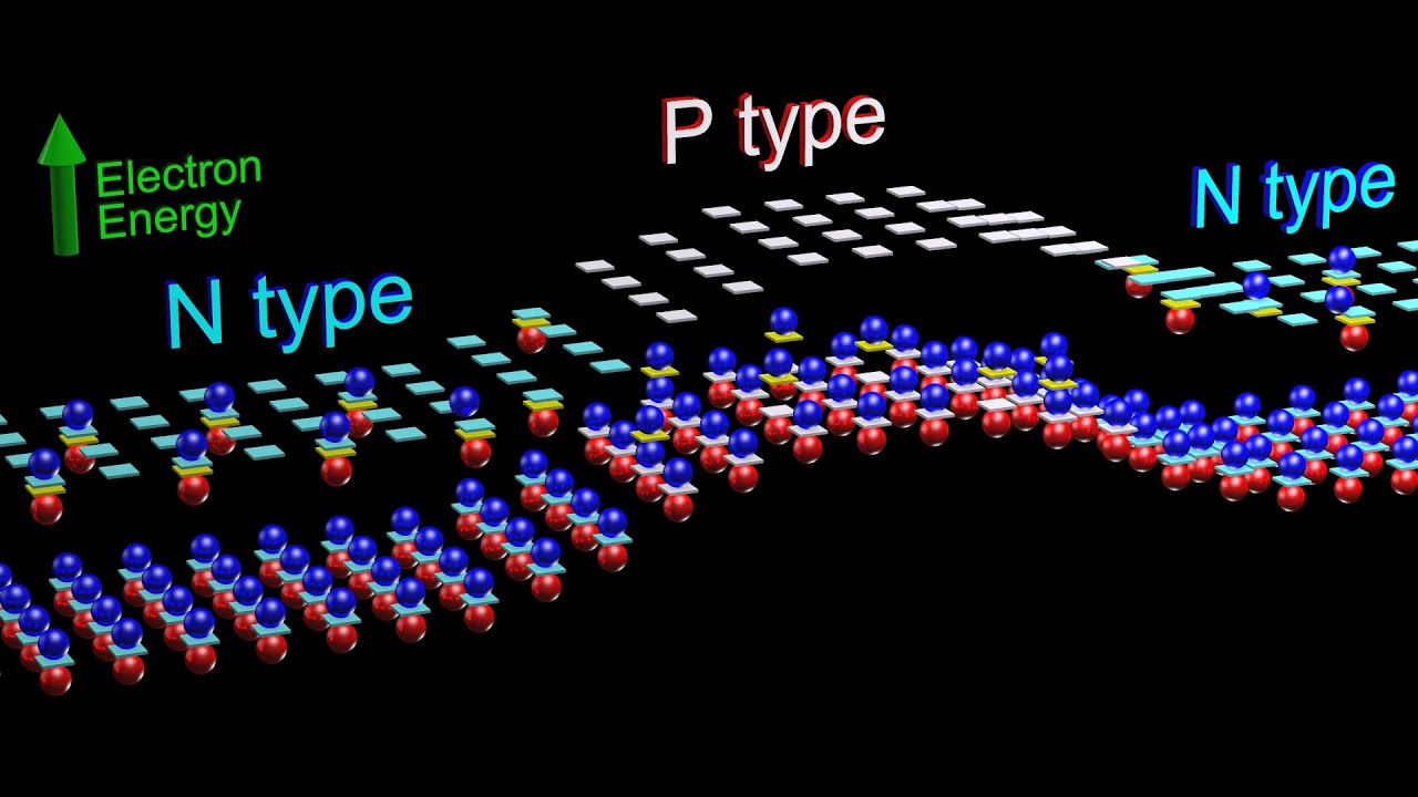
- 🌗 The PN junction forms the core of a transistor, with N-type and P-type materials creating a barrier that can be influenced by external voltage.
- 💼 Engineers use doping to alter silicon's properties, creating N-type and P-type semiconductors that are essential for transistor function.
Q & A
What is the significance of the transistor in the field of electronics?
-The transistor is one of the most important devices ever invented, playing a crucial role in modern electronics due to its ability to act as a switch and amplify signals, which are fundamental functions in controlling and processing electrical currents in circuits.
What are the two main types of transistors mentioned in the script?
-The two main types of transistors mentioned are bipolar and field-effect transistors, with the script primarily focusing on the bipolar version.
What are the two primary functions of a transistor?
-A transistor can act as a switch to control circuits and also amplify signals, making it a versatile component in electronic devices.
Why are higher power transistors often enclosed in a metal case?
-Higher power transistors are enclosed in a metal case to help dissipate the heat generated during operation, which is crucial to prevent damage to the internal components over time.
What is the purpose of attaching metal body transistors to a heat sink?
-Heat sinks are used to enhance the heat dissipation from metal body transistors, ensuring that the components do not overheat and maintain their performance and longevity.
What information can be found on the body of a transistor?
-The body of a transistor typically has text indicating the part number, which can be used to reference the manufacturer's datasheet for detailed specifications and ratings of the transistor.
What are the three pins of a transistor labeled as, and what do they represent?
-The three pins of a transistor are labeled as E for emitter, B for base, and C for collector, representing the different points of electrical connection within the transistor.
Why is it important to check the manufacturer's datasheet for a transistor?
-The manufacturer's datasheet provides essential information about the transistor's voltage and current ratings, ensuring that it is used safely and within its operational limits.
What is the minimum voltage typically required to turn on a transistor?
-Typically, at least 0.6V to 0.7 volts is required to be applied to the base pin for the transistor to turn on and start conducting current in the main circuit.
How does a transistor act as an amplifier?
-A transistor acts as an amplifier by using a small voltage and current at the base pin to control a larger voltage and current in the main circuit, thus amplifying the input signal.
What is the current gain of a transistor, and how can it be determined?
-The current gain of a transistor, symbolized by beta, is the ratio of the collector current to the base current. It can be found in the manufacturer's datasheet or calculated using the formula beta = collector current / base current.
What is the difference between NPN and PNP transistors in terms of current flow?
-In an NPN transistor, the current combines as it flows from the emitter through the base to the collector. In contrast, in a PNP transistor, the current divides, flowing out of the emitter, through the base, and out of the collector.
How are the symbols for transistors represented in electrical drawings?
-Transistors are represented with symbols that include an arrow pointing in the direction of conventional current flow, indicating how they should be connected in circuits.
What is the analogy used in the script to explain the working principle of an NPN transistor?
-The script uses the analogy of water flowing through a pipe with a swing gate in a smaller pipe to explain how an NPN transistor works, where the gate represents the base controlling the flow in the main pipe, analogous to the base controlling the current flow in the transistor.
What is the role of doping in semiconductor materials like silicon?
-Doping is the process of adding impurities to pure silicon to change its electrical properties. P-type doping introduces materials with fewer valence electrons, creating 'holes', while N-type doping introduces materials with extra valence electrons, creating free electrons, which influences the semiconductor's conductivity.
How does the PN junction form in a semiconductor, and what is the depletion region?
-The PN junction forms when P-type and N-type semiconductor materials are joined together. At the junction, a depletion region is created where excess electrons from the N-side move to occupy holes on the P-side, forming a barrier with a built-up charge on either side, which creates an electric field preventing further movement of charge carriers.
What happens when a forward bias is applied to a PN junction?
-When a forward bias is applied to a PN junction, the voltage source causes the barrier to collapse, allowing electrons to flow from the N-type side to the P-type side, enabling current to flow through the junction.
What is the purpose of the emitter in an NPN transistor during operation?
-In an NPN transistor, the emitter's role is to provide a large number of excess electrons due to heavy doping, which, when a forward bias is applied, rushes across to fill the space within the P-type material, initiating the transistor's conduction process.
Outlines
🔌 Introduction to Transistors and Their Functions
This paragraph introduces the transistor as a pivotal invention in electronics, highlighting its two main types: bipolar and field effect, with a focus on the bipolar type. Transistors serve as switches to control circuits and as amplifiers for signals. The physical construction of transistors, including low and high power versions, is discussed, along with the importance of heat dissipation for high power transistors. The paragraph also explains the labeling of the transistor's pins (E for emitter, B for base, C for collector) and the significance of consulting the manufacturer's datasheet for voltage and current ratings. The concept of using a transistor to automate the control of a light circuit is introduced, demonstrating the transistor's ability to allow current flow with a small voltage applied to the base pin.
🔧 Understanding Transistor Operation and Amplification
The second paragraph delves into the operational aspects of transistors, explaining how a small voltage at the base pin can control a larger current in the main circuit, thus acting as a switch or an amplifier. It provides an example of a simple circuit with a LED and a 9V power supply to illustrate the transistor's behavior at different voltage levels. The paragraph also introduces the concept of current gain, denoted by beta, and how it can be found in the manufacturer's datasheet. The difference in current flow between the base and collector pins is emphasized, showcasing the transistor's ability to amplify signals with minimal current input.
🔄 Exploring NPN and PNP Transistors and Their Current Flow
This paragraph discusses the two main types of bipolar transistors: NPN and PNP, explaining their physical similarities and the necessity to differentiate them through part numbers. It describes the current flow in both types when a switch is pressed, highlighting the difference in current direction and how it affects the circuit's operation. The paragraph also explains the concept of conventional current flow versus electron flow, emphasizing the importance of using conventional current in circuit design despite electrons actually flowing in the opposite direction. The explanation includes a comparison of how current combines in an NPN transistor versus how it divides in a PNP transistor, using a simplified example to illustrate the point.
🌐 Semiconductors, PN Junctions, and Transistor Construction
The final paragraph explores the atomic structure of conductors and insulators, leading into an explanation of semiconductors like silicon and how they can be manipulated through doping to create P-type and N-type materials. It describes the formation of a PN junction and the creation of a depletion region, which acts as a barrier to electron flow. The paragraph then explains how these concepts apply to the construction of NPN and PNP transistors, detailing the layers of N and P type materials and their roles within the transistor. The explanation of how a forward bias collapses the barrier and allows current to flow, and how a reverse bias affects the flow of electrons and holes, concludes the discussion on transistor operation.
Mindmap
Keywords
💡Transistor
💡Bipolar Transistor
💡Field Effect Transistor (FET)
💡Switch
💡Amplifier
💡Emitter
💡Base
💡Collector
💡Current Gain (Beta)
💡PNP and NPN Transistors
💡Doping
Highlights
Transistors are one of the most important devices ever invented, with the ability to act as a switch and amplify signals.
There are two main types of transistors: bipolar and field effect, with a focus on bipolar in this video.
Transistors come in various shapes and sizes, with different cases for low and high power applications.
Higher power transistors often have a metal case to dissipate heat, which is crucial for component longevity.
Transistors are labeled with three pins: E for emitter, B for base, and C for collector.
The part number on the transistor body is essential for referencing the manufacturer's datasheet.
Transistors are rated for specific voltage and current levels, which are detailed in their datasheets.
A small voltage applied to the base pin can control the flow of current in the main circuit, acting as a switch.
Transistors can be used to automate control circuits, removing the need for manual switches.
A minimum voltage of 0.6V to 0.7V is typically required to turn on a transistor.
Transistors can amplify signals, as a small change in base pin voltage can significantly alter the main circuit.
The current gain of a transistor, symbolized by beta, is the ratio of collector current to base current.
There are two types of bipolar transistors: NPN and PNP, which differ in their internal doping and current flow.
NPN transistors have the main and control circuits connected to the positive of the battery, while PNP transistors have the emitter connected to the positive.
Transistors are represented with specific symbols on electrical diagrams, with the arrow indicating the emitter.
The operation of a transistor can be likened to a water flow control mechanism, with a small flow controlling a larger one.
Transistors work on the principle of conventional current, despite electrons actually flowing in the opposite direction.
The PN junction in a transistor creates a barrier that can be overcome by applying a specific voltage.
Doping silicon with different materials creates N type and P type semiconductors, which are used in transistor construction.
The internal structure of an NPN transistor consists of two N type layers and one P type layer, with specific doping levels.
The operation of a transistor involves the movement of electrons and the creation of a depletion region at the PN junction.
The video concludes with an invitation to continue learning about electronics engineering through further videos.
Transcripts
This is a transistor
It is one of the most important devices ever
to be invented.
So, we're going to learn how they work in detail in this video.
What is a transistor?
Transistors come in many shapes and sizes.
There are two main types, the bipolar and the field effect.
We're going to mostly focus on the bipolar version in this video.
Transistors are small electronic components with two main functions.
It can act as a switch to control circuits
and they can also amplify signals.
Small low power transistors are enclosed
in a racing case to help protect the internal parts.
But higher power transistors will have a partly metal case, which is used to help
remove the heat which is generated as this will damage the components over time.
We usually find these metal body transistors
attached to a heat sink, which helps remove the unwanted heat.
For example, inside this DC Bench power supply
We have some mosfet transistors which are attached to very large heat sinks.
Without the heat sink
the components quickly reach 45 degrees Celsius or 113 degrees Fahrenheit.
With a current of just 1.2A.
They will become much hotter as the current increases.
But for electronic circuits with small currents, we can just use these resin body transistors
which do not require a heat sink.
On the body of the transistor.
We find some text.
This will tell us the part number which we
can use to find the manufacturers datasheet.
Each transistor is rated to handle
a certain voltage and current, so it is important to check these sheets.
Now with the transistor we have three pins labelled E, B and C.
This stands for the emitter, the base and the collector.
Typically with these resin body type TRANSISTORS
with a flat edge,
the left pane is the emitter,
the middle is the base, and the right side is the collector.
However, not all transistors use this configuration.
So do check the manufacturers datasheet.
We know that if we connect a light bulb to a battery, it will illuminate.
We can install a switch into the circuit
and control the light by interrupting the power supply.
But this requires a human to manually control the switch.
So how can we automate this?
For that, we use a transistor.
This transistor is blocking the flow of current.
So the light is off.
But if we provide a small voltage to the base pane in the middle,
it causes the transistor to start allowing current to flow in the main circuit.
So the light turns on.
We can then place a switch on the controlling pin to operate it remotely
or we can place a sensor on this to automate the control.
Typically, we need to apply at least 0.6V
to 0.7 volts to the base pin for the transistor to turn on.
For example, this simple transistor circuit
has a red LED and a nine volt power supply across the main circuit.
The base pin is connected to the DC Bench power supply
The circuit diagram looks like this.
When the supply voltage to the base pin is
0.5V the transistor is off.
So the LED is also off
at 0.6V the transistor is on, but not fully.
The LED is dim because the transistor is not yet letting the full current flow
through the main circuit.
Then at 0.7V the lead is brighter because the transistor is letting almost the full current through.
At 0.8V, the LED is at full brightness.
The transistor is fully open.
So what's happening is we're using a small
voltage and current to control a larger voltage and current.
We saw that a small change to the voltage on the base pin
causes a large change on the main circuit.
Therefore, if we input a signal to the base pin,
the transistor acts as an amplifier.
We could connect a microphone which varies
the voltage signal on the base pin, and this will amplify a speaker in the main circuit
to form a very basic amplifier.
Typically, there is a very small current on the base pin,
perhaps just 1mA or even less.
The collector has a much higher current, for example, 100mA.
The ratio between these two is known as the current gain and uses the symbol beta
We can find the ratio in the manufacturers datasheet.
In this example, the collector current is 100mA
and the base current is 1mA.
So the ratio is 100mA divided by 1mA, which gives us 100.
We can also rearranges formula to find the currents also.
NPN and PNP transistors
We have two main types of bipolar transistors,
the NPN and the PNP type, the two transistors look nearly identical.
So we need to check the part number to tell which is which.
With an NPN transistor.
We have the main circuit and the control circuit.
Both are connected to the positive of the battery.
The main circuit is off until we press the switch on the control circuit.
We can see the current is flowing through both wires to the transistor.
We can remove the main circuit and the control circuit lED
will still turn on when the switch is pressed
as the current is returning to the battery through the transistor.
In this simplified example,
when this switch is pressed, there are 5mA flowing into the base pin.
There are 20mA flowing into the collector pin
and 25mA flowing out of the emitter.
The current therefore combines in this transistor
With a PNP transistor.
We again have the main circuit and the control circuit,
but now the emitter is connected to the positive of the battery.
The main circuit is off until we press the switch on the control circuit.
We can see with this type that some of the current flows out of the base pin and returns to the battery.
The rest of the current flows through
the transistor and through the main led and then back to the battery.
If we remove the main circuit, the control circuit, LED will still turn on.
In this example, when the switch is pressed,
there are 25mA flowing into the emitter,
20mA flowing out of the collector and 5mA flowing out of the base.
The current, therefore, divides in this transistor
I'll place these side by side so you can see how they compare.
Transistors are shown on electrical drawings
with symbols like these, the arrow is placed on the emitter.
The arrow points in the direction
of conventional current so that we know how to connect them into our circuits.
How does a transistor work
To understand how a transistor works,
I want you to first imagine water flowing through a pipe.
It flows freely through the pipe until we block it with a disc.
Now, if we connect a smaller pipe into the main one and place a swing gate
within this small pipe, we can move the disc using a pulley.
The further the swing gate opens,
the more water is allowed to flow in the main pipe.
The swing gate is a little heavy,
so a small amount of water won't be enough to open it.
A certain amount of water is required to force the gate to open.
The more water we have flowing in this small pipe,
the further the valve opens and allows
more and more water to flow in the main pipe.
This is essentially how an NPN transistor works.
You might already know that when we design electronic circuits,
we use conventional current.
So in this NPN transistor circuit,
we assume that the current is flowing from the batteries positive
into both the collector and the base pin and then out of the emitter pin.
We always use this direction to design our circuits.
However, that's not what's actually occurring.
In reality, the electrons are flowing
from the negative to the positive of the battery.
This was proved by Joseph Thompson, who carried out some experiments
to discover the electron and also prove they flowed in the opposite direction.
So in reality,
electrons flow from the negative into the emitter and then out
of the collector and the base pin. We call this electron flow.
I'll place the side by side so you can see the difference in the two theories.
Remember, we always design circuits using the conventional current method.
But scientists and engineers know that electron flow is how it actually works
by the way, we have also covered how
a battery works in detail in our previous video.
Do you check that out
links can be found in the video description down below.
OK, so we know that electricity is the flow of electrons through a wire.
The copper wire is the conductor and the rubber is the insulator.
Electrons can flow easily through
the copper, but they can't flow through the rubber insulator.
If we look at this basic model of an atom
of a metal conductor, we have the nucleus at the centre and this
is surrounded by a number of orbital shells which hold the electrons.
Each shell holds a maximum number
of electrons, and an electron needs to have a certain
amount of energy to be accepted into each shell.
The electrons located furthest away from the nucleus hold the most energy.
The outermost shell is known as the valence shell.
A conductor has between one and three electrons in its valence shell.
The electrons are held in place by the nucleus,
but there is another shell known as the conduction band.
If an electron can reach this, then it can break free from the atom
and move to other atoms. With a metal atom such as copper.
The valence shell and the conduction band overlap,
so it's very easy for the electrons to move
with an insulator the outermost shell is packed.
There's very little to no room for an electron to join.
The nucleus has a tight grip
on the electrons and the conduction band is far away.
So the electrons can't reach this to escape.
Therefore, electricity cannot flow through this material.
However, there's another material known as a semiconductor.
Silicon is an example of a semiconductor.
With this material,
there's one too many electrons in the valence shell for it to be a conductor.
So it acts as an insulator.
But as the conduction band is quite close,
if we provide some external energy, some electrons will gain enough energy
to make the jump into the conduction band and become free.
Therefore, this material can act as both an insulator and a conductor.
Pure silicon has almost no free electrons.
So what engineers do is dope the silicon
with a small amount of another material which changes its electrical properties.
We call this P type and N type doping.
We combine these materials to form the PN junction.
We can sandwich these together to form an NPN or PNP transistor.
Inside the transistor we have
the collector pin and the emitter pin
between these in an NPN transistor,
we have two layers of N type material and one layer of P type.
The base wire is connected to the P type layer
in a PNP transistor this is just configured the opposite way.
The entire thing is enclosed in a resin to protect the internal materials.
Let's imagine the silicon hasn't been doped yet,
so it's just pure silicon inside.
Each silicon atom is surrounded by four other silicon atoms.
Each atom wants eight electrons in its valence shell
but the silicon atoms only have four electrons in their valence shell,
so they sneakily share an electron
with their neighbouring atom to get the 8 desire.
This is known as covalent bonding.
When we add the N type material such as phosphorus,
it will take the position of some of the silicon atoms.
The phosphorus atoms have five electrons in their valence shell.
So as the silicon atoms are sharing electrons to get their desired eight,
they don't need this extra one, which means there's now extra electrons
in the material and these are free to move around
with P type doping we add in a material such as aluminium.
This atom has only three electrons in this valence shell.
It therefore can't provide its four neighbours with an electron to share.
So one of them will have to go without.
This means a hole has been created where an electron can sit and occupy.
We now have two doped pieces of silicon,
one with too many electrons and one we not enough electrons.
The two materials join to form a PN junction.
At this junction we get what's known as a depletion region
in this region some of the excess electrons
from the N side will move over to occupy the holes in the P side.
This migration will form a barrier
with a build up of electrons and holes on opposite sides.
The electrons are negatively charged and the holes are therefore considered positively charged,
so this Build-Up causes a slightly negatively charged region
and a slightly positively charged region.
This creates an electric field
and prevents more electrons from moving across.
The potential difference across this region is typically around 0.7V
when we connect a voltage source across the two ends
with the positive connected to the P type material.
This will create a forward bias and the electrons will begin to flow.
The voltage source has to be greater than the 0.7V barrier.
Otherwise, electrons cannot make the jump
when we reverse the power supply so that the positive is connected to the N type material.
The electrons held in the barrier will be pulled back towards the positive terminal
and the holes will be pulled back towards the negative terminal.
This has caused a reverse bias
in a NPN transistor.
We have two layers of N type material, so we have two junctions and therefore two barriers,
so no current can flow through it ordinarily.
The emitter N type material is heavily doped,
so there are a lot of excess electrons here.
The base P type is lightly doped, so there are a few holes here.
The collector N type is moderately doped,
so there are a few excess electrons here.
If we connect a battery across the base and the emitter with the positive
connected to the P type layer,
this will create a forward bias.
The forward bias causes the barrier to collapse
as long as the voltage is at least 0.7V.
So the barrier diminishes
and the electrons rush across to fill the space within the P type material.
Some of these electrons will occupy a hole
and they will be pulled towards the positive terminal of the battery.
The P type layer is thin
and was lightly doped on purpose so that there is a low chance of electrons falling into a hole.
The rest will remain free to move around the material.
Therefore, only a small current will flow
out of the base pin, leaving an excess of electrons in the pitot material
if we then connect another battery between the emitter and the collector
with the positive connected to the collector,
the negatively charged electrons within the collector
will be drawn to the positive terminal, which causes a reverse bias.
If you remember, with the reverse bias, the electrons and holes of the barrier are
pulled back across, so the electrons on the P type side
of the barrier are pulled across to the N type side
and the holes on the N type side are pulled back to the P type side.
They are already an excess number of electrons in the P type material.
So they will move to occupy these holes and some of them will be pulled across
because the voltage of this battery is greater.
So the attraction is much higher.
As these electrons are pulled across, they flow into the battery.
So a current develops across the reverse bias junction.
A higher voltage on the base pin fully opens the transistor,
which means more current and more electrons moving into the P type layer.
Therefore, more electrons are pulled across the reverse bias.
We also see more electrons flowing
in the emitter side of the transistor compared to the collector side.
OK, that's it for this video,
but to continue learning about electronics engineering, click on one of the videos
on screen now and I'll catch you there for the next lesson.
Don't forget to follow us on Facebook,
Twitter, LinkedIn, Instagram and of course, the engineering mindset .Com.
5.0 / 5 (0 votes)