Introduction
Summary
TLDRThis course introduces Hardware Modeling using Verilog, a language for specifying hardware behavior, functionality, or structure. Over eight weeks, students will explore Verilog's features, learn behavioral and structural design styles, and write test benches for verification. The course covers modeling of combinational and sequential circuits, good practices, and case studies, including processor design. It also provides an overview of the VLSI design process, emphasizing the importance of CAD tools and the impact of Moore's Law on semiconductor advancements.
Takeaways
- 📘 The course is an 8-week introduction to Verilog, a hardware description language used for specifying the behavior or structure of hardware circuits.
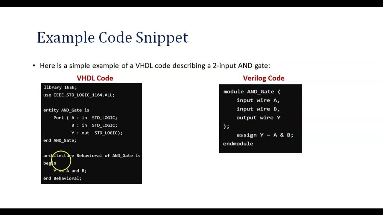
- 🛠️ Verilog allows designers to model functionality in two distinct styles: behavioral and structural, and the course will cover the differences between them.
- 🔍 Students will learn to write test benches for verifying the correctness of hardware designs through simulation.
- 🔌 The course will cover modeling of both combinational and sequential circuits, essential for understanding digital logic design.
- 🛡️ Good practices and avoidable practices in Verilog design will be discussed to enhance the quality of the designs.
- 💡 Case studies, including the design of a complete processor, will be used to illustrate the application of Verilog in complex hardware design.
- 📈 VLSI design complexity has increased dramatically over the years, moving from hundreds of components to billions of transistors in a single chip.
- 🛑 The manual design of circuits is no longer feasible due to their complexity, necessitating the use of computer-aided design (CAD) tools.
- ⚙️ VLSI design involves balancing conflicting requirements such as reducing area, increasing speed, and lowering energy consumption.
- 📉 Moore's Law, which predicts the doubling of transistors on a chip every 18 months, has held true and continues to drive advancements in semiconductor design.
- 🌐 CMOS technology, including innovations like FinFET, enables the miniaturization of transistors and the continued relevance of Moore's Law.
- 🔩 The VLSI design flow is a standardized procedure that includes steps from specification to hardware manufacturing, heavily reliant on CAD tools and HDLs like Verilog.
Q & A
What is the main focus of the course on Hardware Modeling using Verilog?
-The course focuses on teaching the Verilog hardware description language, its features, syntaxes, and how to utilize them for hardware design, including behavioral and structural design styles.
What are the two distinct ways of modeling the functionality of a circuit mentioned in the course?
-The two distinct ways of modeling the functionality of a circuit are behavioral and structural design styles.
What is a test bench in the context of hardware design?
-A test bench is a piece of code used to verify whether a hardware design is working correctly. It is used to evaluate the results of simulations.
What does the VLSI design process involve?
-The VLSI design process involves a series of steps starting from the specification of the design to the actual hardware circuit fabrication, including synthesis, simulation, layout generation, and testability analysis.
How has the complexity of VLSI circuits evolved over the years?
-The complexity of VLSI circuits has increased dramatically over the years, with an exponential growth in the number of transistors that can be integrated into a single chip, moving from hundreds or thousands to billions.
What is Moore's Law and how does it relate to the semiconductor industry?
-Moore's Law is the observation that the number of transistors on a chip doubles approximately every 18 months, indicating an exponential growth in the semiconductor industry. It has been a driving principle for advancements in chip design and fabrication.
What is the significance of CMOS technology in VLSI design?
-CMOS technology is the most dominant technology used in manufacturing VLSI chips. The shrinking of CMOS transistors has enabled the continued growth in the number of transistors that can be placed on a chip, sustaining Moore's Law.
What is a netlist in the context of hardware design?
-A netlist is a graphical representation where vertices indicate components and edges indicate interconnects, used to specify how different functional blocks are interconnected at various levels of abstraction.
What is the purpose of simulation in the VLSI design flow?
-Simulation is a crucial step in the VLSI design flow for verification purposes. It is used to check and ensure that the Verilog modules meet the design specifications and are functioning as intended.
What are the conflicting requirements that a designer may face during the VLSI design process?
-Designers may face conflicting requirements such as reducing the area, increasing the speed, and minimizing energy consumption. Optimizing one aspect may adversely affect another, making it a challenge to balance these requirements.
What is the alternative to chip fabrication mentioned in the script?
-An alternative to chip fabrication is using a Field Programmable Gate Array (FPGA), which allows for greater flexibility and the ability to program the device directly in the field, although it may offer lower speeds compared to fabricated chips.
Outlines
📘 Introduction to Hardware Modeling with Verilog
This paragraph introduces the course on Hardware Modeling using Verilog, which will span 8 weeks and cover the features of the Verilog language. The course aims to teach designers how to utilize Verilog to model the behavior, functionality, or structure of hardware circuits. It will focus on behavioral and structural design styles, writing test benches for verification, and modeling combinational and sequential circuits. The course will also cover good practices in design and conclude with a case study on designing a complete processor using Verilog, including the data and control paths. The lecture begins with an overview of the VLSI design process and the importance of hardware description languages in modern chip design.
🚀 VLSI Design Complexity and CAD Tools
The second paragraph delves into the complexity of VLSI design and the necessity of computer-aided design (CAD) tools due to the exponential growth in the number of transistors on chips. It discusses the conflicting requirements designers face, such as reducing area, increasing speed, and lowering energy consumption, which are often not independently controllable. The paragraph also touches on the standardization of design flow and the emphasis on low power design and increased performance. It provides a historical perspective on the development of ICs, from simple planar ICs to modern complex chips like the Intel Quad Core Nehalem series processor, and introduces Moore's Law, which predicts the exponential increase in transistor count on chips over time.
📈 Sustaining Moore's Law with Advances in Semiconductor Technology
This paragraph continues the discussion on Moore's Law, highlighting the skepticism and the continuous advancements in semiconductor fabrication that have allowed for its sustenance. It presents a graph illustrating the exponential growth in the number of transistors from 1970 to 2015, with examples of processors from Intel and other manufacturers. The paragraph also explains the technological advancements that have made this growth possible, such as the shift from traditional CMOS to FinFET technology, which allows for more compact transistor design. It concludes with a mention of potential future technologies like quantum computing.
🛠️ VLSI Design Flow and the Role of Hardware Description Languages
The fourth paragraph outlines the VLSI design flow, which is a standardized set of procedures for creating a VLSI circuit or chip. It covers the steps from specification to hardware circuit manufacturing, emphasizing the reliance on computer-aided design tools due to the complexity of modern designs. The paragraph introduces hardware description languages (HDLs) as the foundation for these tools, allowing designers to specify and transform designs at various levels of abstraction. It also mentions the transformation process from behavior to register transfer level, gate level, transistor level, and finally, layout level, before fabrication.
🔍 Steps in the Design Flow and Synthesis Process
This paragraph provides a detailed look at the steps involved in the design flow, starting from behavioral design expressed in HDLs like Verilog or VHDL. It explains the transformation process through synthesis, where the design is translated into more detailed specifications, ultimately leading to hardware. The paragraph discusses data path design at the register transfer level, the creation of netlists representing components and interconnects, and the use of standard cells in logic design. It also touches on the challenges of optimizing design to meet conflicting requirements such as minimizing gate count, delays, and power consumption.
🌐 Physical Design, Manufacturing, and Alternatives to Traditional Fabrication
The final paragraph of the script discusses the final stages of the design flow, focusing on physical design and manufacturing. It describes the generation of the final layout containing regular geometric shapes for fabrication on silicon. The paragraph also introduces the concept of field programmable gate arrays (FPGAs) as an alternative to traditional chip fabrication, offering greater flexibility but at the cost of reduced speed. It concludes with a mention of other steps in the design flow, such as simulation for verification, formal verification, and testability analysis, which are important but beyond the scope of the course.
Mindmap
Keywords
💡Verilog
💡Hardware Modeling
💡Behavioral and Structural Design Styles
💡Test Benches
💡VLSI Design Process
💡Moore's Law
💡CMOS Technology
💡FinFET
💡CAD Tools
💡Design Flow
💡Field Programmable Gate Array (FPGA)
Highlights
Introduction to the course on Hardware Modeling using Verilog and its 8-week duration.
Discussion on the features of Verilog for hardware design and optimization.
Exploration of behavioral and structural design styles in Verilog.
Importance of writing test benches for design verification.
Learning objectives including modeling combinational and sequential circuits.
Highlighting good practices and avoidable practices in hardware design.
Case study on designing a complete processor using Verilog.
Overview of the VLSI design process and its significance.
Dramatic increase in VLSI circuit complexity and the role of fabrication technology.
Necessity of computer-aided design (CAD) tools due to circuit complexity.
Conflicting design requirements such as area, speed, and energy consumption.
Standardization of design flow in VLSI circuit creation.
Moore's Law and its prediction of exponential growth in semiconductor industry.
Technological advancements like CMOS and FinFET that sustain Moore's Law.
VLSI design flow as a standardized set of procedures from specification to hardware.
Reliance on hardware description languages for CAD tools in design transformation.
Transformation of behavioral design into register transfer level and logic design.
Different levels of netlist specification in the design process.
Role of standard cells in logic design and their optimization.
Physical design and manufacturing steps leading to final hardware creation.
Alternative approach of using FPGA for design prototyping and its trade-offs.
Importance of simulation for verification at various levels of design.
Conclusion summarizing the course content and VLSI design flow understanding.
Transcripts
Welcome to the course on Hardware Modeling using Verilog. Now in this course over the next 8 weeks,
we shall be discussing the various features of the Verilog hardware description language,
and see that how as a designer you can utilize the facilities and the
features that are they are as the part of the language to the best possible extent.
So, today we start with some of the basic introductory topics.
So, let us start by talking about the main objectives of this course. So,
as you know the name of this course is hardware modeling using Verilog. Now Verilog
is one of the so-called hardware description languages that you may already be knowing,
it is a language using which a designer can specify the behavior, or the functionality,
or the structure of some given hardware; some specified hardware circuit. Now in this as part of
this course well we shall of course, be learning about the Verilog hardware description language,
its various features, the syntaxes, and so on. Specifically, we shall be looking at,
two different distinct way of modeling the functionality of a circuit this so-called
behavioral and the structural design styles. So, we shall be explaining the differences. And from
the point of view of verifying whether the design is correctly working or not,
its correct or not, we have to write something called test benches, or test harness.
So, we shall also see how to write such test benches and evaluate the results of simulations,
we shall be learning about modeling both combinational and sequential circuits. And
during the course of this we shall be learning also what are the good practices and what are
the so-called avoidable practices that a designer should be aware off. And of course,
we shall be looking at some of the case studies. Specifically, at the end we shall be looking at
the design of a complete processor and we see how using Verilog, we can design the data path and
also the control path of the processor, ok. So, we start by talking a few things about the
VLSI design process. Because you see whenever you are talking about a hardware description language,
you are directly or indirectly talking about some piece of hardware which you are trying to
design. Now, the first and the most natural kind of hardware building block that comes to our mind
is a chip, it is an IC. So, today we are in the area of very large-scale integration or VLSI,
so we talk about a VLSI chip as our basic hardware building block.
So, when you talk about the VLSI design process there are a few things that we need to keep in
mind. First thing is that over the years the complexity of VLSI circuits and consequently the
design, they have increased dramatically. So, means when I say it is increase dramatically,
means in fact there has been an exponential increase over the years. I shall show you a
slide just depicting the kind of increase that has taken place. But the point to notice that earlier
few decades back we use to design some chips, which consisted or contained few 100 or 1000 of
gates or transistors, but now today we are talking about circuits or chips consisting of billions of
transistors. So, you can just see the difference the dramatic advancements, and improvements
that has been taken place over the years, ok. So, because of this increased size and complexity,
this has been met possible of course because of improvement in the fabrication technology.
The VLSI fabrication technology have improved dramatically. And as a consequence because of
the complexity of the circuits manual design is simply ruled out. So, earlier when the
circuit was smaller you could have designed your circuits on a piece of paper layout,
on a piece of graph paper and so on and so forth, but now when we are talking about millions and
billions of transistor you have to make use of a computer system and use some so-called
computer aided design tools ok the CAD tools. And in the process there is some conflicting
requirements that often come, in front of the designer. Like for example, the designer may
want to reduce the area, the designer may want to increase the speed, the designer
may also want to reduce the energy consumption, because as you know most the circuits today are
working on battery. So, it is quite natural to try and conserve the power or the energy
in the battery for a longer period of time. So, it is very important to come up with some
design ideas or principles that will consume less energy, right. But often these requirements are
conflicting. When you try to reduce area may be your delivery increase, may be if you want to
reduce the power, your area will increase and so on. So, these requirements are not independently
controllable. If you try to optimize one you may make the other one worse, right.
So, the present trend is to standardize something called design flow means that
steps that you need to follow to create a VLSI circuit or a chip. And as I said the present
emphasis is number 1 on low power design and number 2 on increased performance.
So, here in this diagram I am showing 2 circuits side by side. So, on the left
you have the first IC planar means it is laid down in a single plain this is called a planar IC. So,
you can very easily see the connections the metals and the devices which are prepared,
this was a very simple circuit. And on the right side you think of one of the;
you see one of the modern processor chips the Intel Quad Core Nehalem series processor. So,
here as I said you have something of the order of billion transistors packed in a single chip.
So, when you look at the layout in a very compacted way you see a colorful picture
like this, where of course the different colors indicate the different layers
of the circuit, right, Ok, this is a very interesting plot, Moore
s Law is a very important law in semiconductor design you can say. The persons who are into
semiconductor design, they all know about Moore s Law. There was a person called Gordon Moore
who as early as in the 1960s predicted some behavior about the growth in the semiconductor
industry. So, what he had said at that time was that the number of transistors that you can put
inside the chip would be increasing exponentially with time, with the number of years that pass.
So, there have been some refinements to this basic you can say law or postulate. So, what
it is accepted more or less today is something like this it says that every 18 months or so
the number of transistors in a chip single chip will get doubled. Now, there were people who had
doubted this principle or law since quite a long time in the past. This said that well the devices
are becoming smaller and smaller the transistors you are making smaller, so there will be a time,
a time will come where you will not be able to make the devices any further smaller.
So, there will be a limit and beyond that Moore s Law will cease to exist. But actually
what has happened till today is that, because of semiconductor fabrication advances we are able to
fabricate bigger chips, in the process we have been able to sustain Moore s Law, we have been
put more circuits in the chip. So, if you look at this graph, so on the x axis we are plotting year
started from 1970 so here it shows up to 2015, and on the y axis you see the number of transistors
which is in a log scale see 1000 here up to here it is 1 billion here it is 10 billion. So,
you can see there is a straight line kind of a behavior which indicates exponential growth,
and here the blue dots refer to the processors which are manufactured by the processor major
Intel Corporation, the red dots are the processors manufactured by some other companies, ok.
So, Moore s Law as you can see, this has continued to hold and this trend is still
a straight line behavior which indicates exponential growth over the years.
Well, the technologies that have made this possible are well CMOS. You may be knowing
that CMOS is the most dominant technology today, with which we are manufacturing our VLSI chips,
and the CMOS transistors are becoming smaller and smaller and smaller over the years. There is
something called feature size which we talk about, that is roughly that is equal to this smallest
feature or the transistor that you can fabricate. Well, the state of the art CMOS technology today
you can go down up to 22 nanometer, this is traditional CMOS fabrication. But there
has been some very innovative kind of CMOS designs also, there is something called FinFET,
where the gate drain and the source they are staked vertically instead of horizontally as
in the traditional case, and in this way you can pack transistors in a smaller area.
So, today in the FinFET state of the technology you can go down to 14 nanometer. And many of the
modern chips that are coming in the market, they are actually manufactured using this
FinFET technology, ok. And the picture which is shown in the right, this is of course futuristic,
this we do not have today, tomorrow quantum computer may come so you may be having a
new technology the quantum technology. So, looking at the VLSI design flow again, so what
is a VLSI design flow? VLSI design flow is nothing but a standardized set of design procedure. Means,
here we specify the step by step procedure to be followed starting from our given specification,
what you want to do, down to the actual hardware circuit, that you want to built or manufacture.
This is the overall design procedure. And this typically encompasses many steps,
just a few of them are shown here. Starting from the specification, you go through
some steps called synthesis, simulation, layout generation, testability analysis,
and there are many more steps in between, ok. So, these steps have to be followed before we can
actually get a design fabricated, or manufactured. Now, because of the complexity of design as I said
that we need the help of computers. So, it is just beyond the capability of human being to carry out
the design in a manual way the more. So, you have to rely on computer aided design
tools. And this computer aided design tools today are all based on some hardware description
language. See just like the high level languages like C, C++ or Java we have a set of language,
languages with which we can specify our hardware, and after specifying
that we give it to our CAD tools and the CAD tools will be doing the rest for us, ok.
So, these tools are based on hardware description language as I said. These description languages
they provide ways to represent designs. Not only the initial design, so as the cad tools translate
or transform the designs they will represent this specification at the different steps of
transformation as well, ok this we will see later. So, here is exactly what I was trying to mean. So,
the CAD tool will transform some input which is specified in the hardware description
language and generate an output which will also be a hardware description language,
but the output will contain more detailed information about the hardware than the input.
Like some of the typical steps in the CAD tool transformation as follows. From the behavior
you can translate or transform your design into a register level design, register transfer level
which means from the behavior, you convert it into a form where you have the registers,
counters, adders, multipliers, multiplexers, a design at that level, ok. Now, once you have
done that may be the next step will be to convert each of those functional blocks into gate levels,
then the gate level you convert to the transistor levels, then each transistor you convert to the
final layout level. So, once you have done this your design is ready for fabrication.
So, once you have carried out sufficient analysis and simulation to find out,
that your design is meeting your requirements in terms of power consumption and delay,
you can send it for fabrication. So, there are two computing HDLs today
most popular: so one is Verilog other is VHDL. So, in this course as I have told you we shall
be looking at the language Verilog. Now earlier as I have said that the designs
are created using HDLs, so Verilog or VHDLs are very typical examples of these HDLs.
So, you can specify a design in either Verilog,
or in VHDL and as the CAD tools transformed these designs from one level to the next,
so the transform design is also expressed in similar kind of hardware description languages.
Now, these are not the only ones there are other hardware description languages as well,
some of the popular languages are like SystemC, SystemVerilog and so on,
but here in this course we shall be concentrating only on Verilog.
Talking about the design flow the simplistic view is as follows: starting from a design idea we have
to finally come down to our chip design or a board design. So, we typically start with the behavioral
design which is in the form of a pseudo code in a hardware description language or some kind of
a flow graph notation. So, in the first level of translation we can convert the behavioral
design into something data path design, which is the so-called register transfer level design,
where the basic building blocks are buses, registers, multiplexers, adders, and so on.
Then in the next step we convert it into logic design where you have gates and flip flops,
then physical design where you have transistors, then we go for the last step of manufacturing,
where the transistors are finally laid out and they are ready to be fabricated on silicon.
So, now we can send out designs, to the fabrication house where they can actually
fabricate our chip for us, ok. So, talking about the steps in the design flow,
the first was the behavioral design. As I have said here, we just specify the functionality of
the design in terms of the behavior we do not say, how it is doing it, we just say what we
want. Some examples, in the behavioral style, so we can express a Boolean expression function and
the form of Boolean expression or in the form of a truth table. If it is a sequential circuit we
can express it as a finite state machine: for example, just as a state transition diagram,
or as a state transition table. Or you can even specify it a very high level,
just like a program written C or C++ or Java in a very high level of abstraction you can write a
pseudo code just in the form of an algorithm. Now, during the design flow the steps, this
behavioral design have to be transformed which is called synthesis, synthesized in to more detailed
specification as a result of which you will be finally getting your hardware.
So, data path design as I said here, we talk about register transfer level components like registers,
adders, multipliers, multiplexers, decoders, bus etc. Now, when you call a netlist,
netlist is nothing but some kind of a graph where the vertices indicate components
and the edges indicate interconnects. Like you think of a graph where there are some
vertices and there are some edges. So, when you say netlist I have a number of such blocks, and I
also specify how these blocks are interconnected. Now, this blocks can be at various different
levels. Now, this block can be very high level, high level like, it can be adder,
it can be a gate, it can be a transistor for example. So, I can specify a netlist at various
different levels of abstraction, right. So, whenever we specify a netlist this kind of a
design specification is also referred to as a structural design. Now, this term we shall be
using repeatedly when we will be discussing some details about Verilog in the next classes. So,
netlist as I said, it can be specified at various levels, functional level, gate level, transistor
level and so on. And during the synthesis process there will be systematically transformed
from one level to the next, right. Now, when you come to the logic design level,
now here we have here again a netlist but now your blocks are gates and flip flops, or something
called standard cells. Standard cell like, what is standard cell we should discuss it later. Well a
standard cell basically is a pre designed circuit module like, it can be gates, and flip flops,
small circuit like a multiplexer, whose layout is already given to you. So, you have this
standard cell already present in a library, so in your design if you want you can pick up one
of those standard cell you can put them in your layout directly, ok. In that way you create your
layout and this standard cell library contains the most commonly used small functional modules
in a highly optimized layout form, fine. And in this type of logic design, various
logic optimization techniques are used to minimize your design, to create a so-called cost effective
design as far as possible, ok. Now, as I said earlier that during this process there can be
some conflicting requirements, like minimizing number of gates, minimizing delays, that means,
number of gate levels, minimizing powers, which means number of signal transitions that
are taking place at the outputs of the gates. Now, these requirements are often conflicting,
if you want to minimize one of these, possibly the others can increase, right, so this is
something that you have to keep in mind. And lastly physical design and manufacturing:
here, the final layout that is to be sent for fabrication is generated. Now,
at this level the layout will contain a large number of regular geometric shapes,
because ultimately when you are going for fabrication, you are actually fabricating
some patterns on the surface of silicon: metal layer, poly silicon layer, diffusion layer,
and all of them have regular polygonal shapes, that polygons typically rectangles. So, at this
level your specification will consist of a very large number of such regular polygonal shapes.
Or suppose you do not want to go for a chip to be fabricated as an alternative, you can also go for
something called a field programmable gate array, or FPGA, where from the design you can directly
program the device which can be done in field in your laboratory, and as a result you can have much
greater flexibility. But as compared to a chip you are fabricating, here the speed will be less, ok.
This is the trade off you have to realize. So, there are some other steps in the design flow
also, these are not the only ones. Like simulation is very important step for verification. Like for
example in this course we shall be extensively using simulation to check and verify the Verilog
modules that we will be writing. Ok, we will also be informing you telling you
how to do this simulation so that you can do or carry out the simulation yourself, right.
So, this simulation can be carried out at various levels of specification, logic level, transistor
level, circuit level and so on. There is a step called formal verification, of course this
will be beyond the scope of this course, where using some mathematical and formal techniques,
you can check whether your designs are meeting the specifications or not. And again testability
analysis test pattern generation is also very important. So, when you manufacture or designs
some hardware, you will also have to test whether your final manufactured hardware is working
correctly or not. Again this step is beyond the scope of this course we shall not be also
talking about testability and testing here, ok. So, with this we come to the end of this first
lecture. In this lecture we have basically tried to give you an overview about what are
the things we are expected to cover in this course and some basic concepts of VLSI design
flow. Because understanding the VLSI design flow the process that is embedded there in, it will
allow you to have a better understanding of how you can create a design using a so-called HDL,
it can be either Verilog or VHDL as I said, so that the final hardware that will be generated
in the process can be better in some sense. So, over the course of this lectures that will follow,
we shall being trying to address these issues. Thank you.
5.0 / 5 (0 votes)