Chapter 2 Homog Semicon Fundamentals and Band Structures
Summary
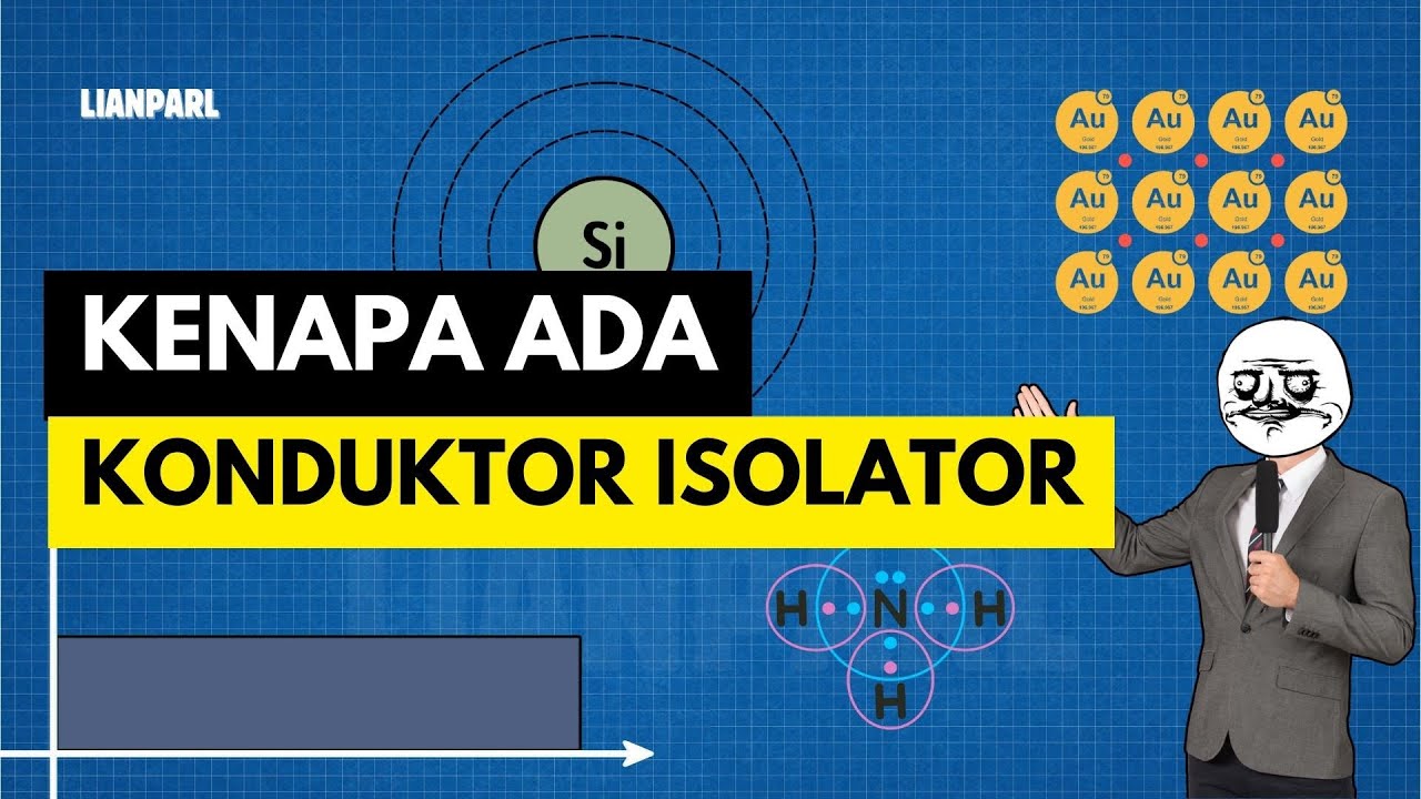
TLDRThis video covers the fundamentals of semiconductors, focusing on their band structure and electrical conductivity. It explains how atoms bond through covalent (calent) bonding, creating the energy bands: the valence band and conduction band, with the gap between them known as the band gap. The size of the band gap determines a material's conductivity, with insulators having a large gap, semiconductors a smaller gap, and metals having overlapping bands. The video also discusses charge carriers, such as electrons and holes, and their role in semiconductor conductivity, highlighting the differences between materials like silicon, germanium, and gallium arsenide.
Takeaways
- 😀 A semiconductor is a material that has electrical conductivity between an insulator and a metal, and its conductivity can change based on external conditions.
- 😀 Semiconductors have a bonding structure called 'covalent bonding' where atoms share valence electrons to form stable configurations.
- 😀 The energy levels in a semiconductor are divided into two main bands: the conduction band (higher energy) and the valence band (lower energy).
- 😀 The band gap is the energy difference between the conduction band and the valence band. Electrons need energy to jump from the valence band to the conduction band.
- 😀 The band gap is crucial in determining a material's electrical conductivity. A smaller band gap means a material is more conductive.
- 😀 Semiconductors, unlike insulators, have a smaller band gap, making it easier for electrons to jump to the conduction band and thus conduct electricity.
- 😀 Metals have overlapping conduction and valence bands, meaning they always have free electrons available to conduct electricity.
- 😀 The energy gap of different semiconductors varies, affecting their conductivity. For example, Germanium has a smaller band gap compared to Silicon and Gallium Arsenide, making it the most conductive.
- 😀 The conductivity of a semiconductor is also determined by the presence of current carriers—electrons in the conduction band and holes in the valence band.
- 😀 Insulators have the widest band gaps, making it extremely difficult for electrons to move to the conduction band, thus they do not conduct electricity.
- 😀 Understanding the band gap and energy levels of a semiconductor is essential for designing and using semiconductors in electronic devices like transistors.
Q & A
What is the definition of a semiconductor?
-A semiconductor is a material with electrical conductivity that is higher than an insulator but lower than a metal. Its conductivity can vary depending on the conditions, such as temperature or applied voltage.
What is covalent bonding in semiconductors?
-In covalent bonding, neighboring atoms share their valence electrons to achieve a stable configuration. In semiconductors like silicon, each atom shares electrons with four neighboring atoms, creating a stable outer electron shell.
What are the two main energy bands in a semiconductor?
-The two main energy bands in a semiconductor are the **Valence Band (EV)**, where electrons are tightly bound to atoms, and the **Conduction Band (EC)**, where electrons have enough energy to move freely and conduct electricity.
What is the band gap in a semiconductor?
-The band gap (EG) is the energy difference between the Valence Band and the Conduction Band. It represents the amount of energy needed for an electron to jump from the Valence Band to the Conduction Band.
What is the Forbidden Gap in a semiconductor?
-The Forbidden Gap is the energy range between the Valence Band and the Conduction Band where no electrons are allowed to exist. This gap is also referred to as the band gap.
How is electrical conductivity related to the band gap?
-The electrical conductivity of a material is inversely related to the size of its band gap. Materials with a smaller band gap, like semiconductors, can conduct electricity more easily than materials with a large band gap, like insulators.
What are the key differences between insulators, semiconductors, and metals?
-Insulators have the widest band gaps, preventing electron movement and making them poor conductors. Semiconductors have narrower band gaps, allowing electrons to move into the Conduction Band under specific conditions, making them moderate conductors. Metals have overlapping Valence and Conduction Bands, allowing free electrons to always conduct electricity.
Why is germanium considered a more conductive semiconductor compared to silicon and gallium arsenide?
-Germanium has the smallest band gap (0.66 eV) among the materials mentioned, making it easier for electrons to jump from the Valence Band to the Conduction Band, thus it is more conductive than silicon (1.12 eV) and gallium arsenide (1.42 eV).
What are the two types of charge carriers in a semiconductor?
-The two types of charge carriers in a semiconductor are **electrons**, which carry negative charge and move in the Conduction Band, and **holes**, which represent the absence of electrons in the Valence Band and contribute to conductivity by moving in the opposite direction to the electrons.
How does external energy (e.g., voltage or bias) influence the conductivity of a semiconductor?
-External energy, such as a voltage or bias, can provide enough energy to excite electrons from the Valence Band to the Conduction Band, allowing the semiconductor to conduct electricity. This is why semiconductors are often used in electronic devices like transistors.
Outlines

This section is available to paid users only. Please upgrade to access this part.
Upgrade NowMindmap

This section is available to paid users only. Please upgrade to access this part.
Upgrade NowKeywords

This section is available to paid users only. Please upgrade to access this part.
Upgrade NowHighlights

This section is available to paid users only. Please upgrade to access this part.
Upgrade NowTranscripts

This section is available to paid users only. Please upgrade to access this part.
Upgrade Now5.0 / 5 (0 votes)


