The 3-D Transistor Transition
Summary
TLDRThe semiconductor industry underwent a significant transformation with the introduction of 3D transistors, specifically the FinFET, starting in 2011. This innovation was essential due to the limitations of traditional planar MOSFETs, which faced issues like leakage and power inefficiency as transistors shrank. The FinFET structure, with its gate wrapping around the channel, improved control and performance while maintaining compatibility with existing manufacturing processes. As the industry evolves, newer architectures like Gate-All-Around are emerging to further enhance transistor capabilities, although the economic feasibility of these advanced technologies remains a critical challenge.
Takeaways
- 😀 The semiconductor industry transitioned to 3D transistors known as FinFETs starting in 2011.
- 😀 Traditional planar transistors, or MOSFETs, faced limitations due to shrinking sizes, leading to increased leakage current.
- 😀 Classical scaling involved shrinking transistor dimensions, improving performance and reducing power consumption.
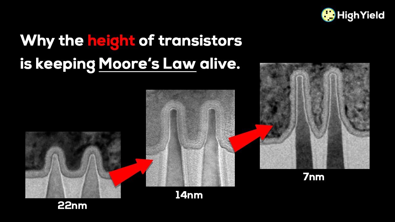
- 😀 The 'short-channel effect' became a significant issue as transistor sizes approached 20 nanometers, complicating power efficiency.
- 😀 DARPA initiated the 25-nm Switch project to explore new transistor structures, leading to innovative proposals from various institutions.
- 😀 FinFET technology enhances gate control over the channel by wrapping around it, improving performance and reducing power leakage.
- 😀 The FinFET has a smaller footprint compared to planar transistors, allowing for more transistors to be placed on a chip.
- 😀 The adoption of strain engineering and High-K metal gates helped improve performance before the full transition to FinFETs.
- 😀 The Tri-Gate transistor, developed from FinFET technology, utilizes three gate layers for enhanced control.
- 😀 New architectures like Gate-All-Around FETs are emerging as FinFETs begin to lose effectiveness, highlighting ongoing innovation in semiconductor technology.
Q & A
What major technical transition did the semiconductor industry undergo starting in 2011?
-The semiconductor industry began producing three-dimensional transistors known as Fin Field-effect Transistors (FinFETs), marking a significant shift from traditional planar transistors.
What is the traditional building block of the semiconductor industry?
-The traditional building block is the Metal-Oxide Semiconductor Field Effect Transistor (MOSFET), commonly used in digital circuits.
What were the limitations of classical scaling in semiconductor technology?
-Classical scaling faced challenges as transistors shrank, leading to issues like the short-channel effect, where control over current flow weakened and resulted in increased power leakage.
What is the 'short-channel effect'?
-The short-channel effect occurs when the source and drain of a transistor are too close, causing current to bypass the gate control and leading to leakage, especially as transistors shrink in size.
What was DARPA's involvement in the development of new transistor technologies?
-In 1996, DARPA called for proposals for research on sub-25 nanometer devices due to concerns over the industry's lack of long-term plans beyond 2002, which led to innovations like the FinFET.
What are the key advantages of the FinFET design compared to traditional planar transistors?
-FinFETs allow the gate to wrap around the channel on three sides, providing better control over current flow, a smaller footprint, and improved power efficiency.
What role did Professor Hu Chenming play in the development of the FinFET?
-Professor Hu led a team at UC Berkeley that proposed the FinFET design, successfully prototyping the device with DARPA's funding, which advanced semiconductor technology.
What are High-K Metal Gates, and why were they introduced?
-High-K Metal Gates replaced the traditional silicon dioxide layer in transistors with a high-K dielectric material, helping to improve gate control and reduce leakage currents.
What challenges did the semiconductor industry face when transitioning to FinFET technology?
-The industry struggled with scaling and yield issues in mass production of FinFETs, leading to delays as they adapted new multi-patterning techniques.
What future architecture is the semiconductor industry exploring beyond FinFETs?
-The industry is moving towards Gate-All-Around (GAA) architecture, which fully surrounds the channel, allowing for even better control and the potential to stack multiple channels.
Outlines

This section is available to paid users only. Please upgrade to access this part.
Upgrade NowMindmap

This section is available to paid users only. Please upgrade to access this part.
Upgrade NowKeywords

This section is available to paid users only. Please upgrade to access this part.
Upgrade NowHighlights

This section is available to paid users only. Please upgrade to access this part.
Upgrade NowTranscripts

This section is available to paid users only. Please upgrade to access this part.
Upgrade NowBrowse More Related Video
TSMC FinFlex: How Chips are made Worse to get Better

2006-2011 Lexus GS.. What You Didn't Know (Facts & Specs)

Transistor hoạt động như thế nào? | Transistor là gì? | Bóng bán dẫn là gì? | Tri thức nhân loại

391 San Antonio Rd.—A Semiconductor Documentary

TSMC 5nm, 3nm and 2nm devices explained | Technology Node | VLSI | Why such naming? | TSMC

Perang Dingin Teknologi Chip Panas Membara! Siapa Menang?
5.0 / 5 (0 votes)