Collector Feedback Bias with Emitter Resistance
Summary
TLDRThis lecture provides a comprehensive overview of collector feedback biasing with emitter resistance, detailing the process of finding the operating point using Kirchhoff's Voltage Law. It explains how to calculate the base and collector currents, emphasizing the importance of ensuring collector current independence from the transistor's beta value. The output voltage is derived through careful analysis of voltage drops in the circuit. The session concludes by introducing voltage divider bias, a key concept that will be explored in the next lecture, encouraging viewers to familiarize themselves with Thevenin's theorem.
Takeaways
- 📚 The lecture focuses on collector feedback biasing combined with emitter resistance.
- 🔍 Determining the operating point is essential for this biasing scheme.
- ⚡ Kirchhoff's Voltage Law (KVL) is applied in the input loop to find the base current (IB).
- 🧮 The KVL equation begins with the supply voltage (VCC) and includes voltage drops across resistors and transistors.
- 📈 The relationship between emitter current (IE), collector current (IC), and base current (IB) is established: IE = (β + 1) × IB.
- 🔗 A derived expression for base current (IB) is given, showing its dependence on VCC, VBE, and resistances.
- 🚦 Collector current (IC) is calculated using the formula IC = β × IB, emphasizing its dependence on β.
- 🔒 A crucial condition is that RB must be smaller than (β + 1)(RC + RE) to keep IC independent of β.
- 🔌 The output voltage (VCE) can be calculated from the equation VCE = VCC - IC × (RC + RE).
- 🔜 The next lecture will cover voltage divider biasing, encouraging a review of Thevenin’s theorem beforehand.
Please replace the link and try again.
Outlines

This section is available to paid users only. Please upgrade to access this part.
Upgrade NowMindmap

This section is available to paid users only. Please upgrade to access this part.
Upgrade NowKeywords

This section is available to paid users only. Please upgrade to access this part.
Upgrade NowHighlights

This section is available to paid users only. Please upgrade to access this part.
Upgrade NowTranscripts

This section is available to paid users only. Please upgrade to access this part.
Upgrade NowBrowse More Related Video
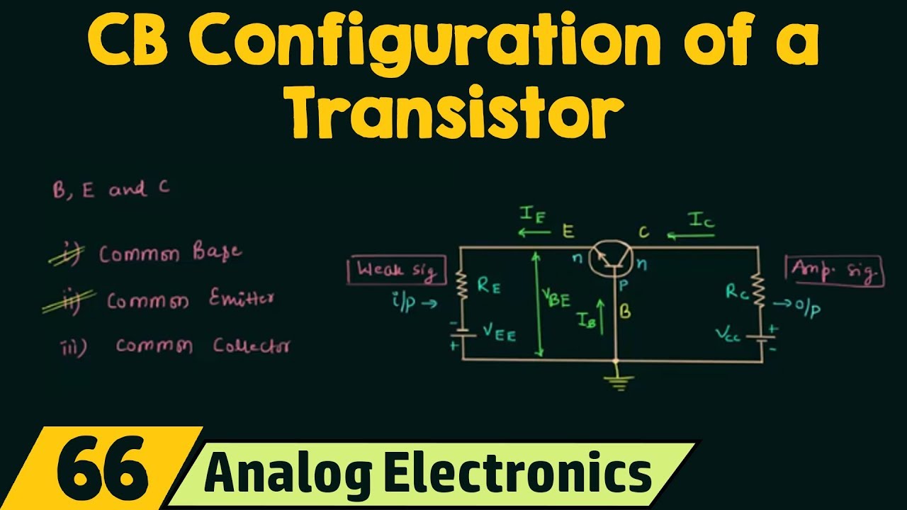
Common-Base Configuration of a Transistor
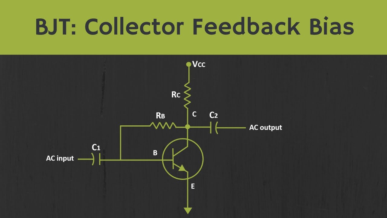
BJT: Collector Feedback Bias Explained
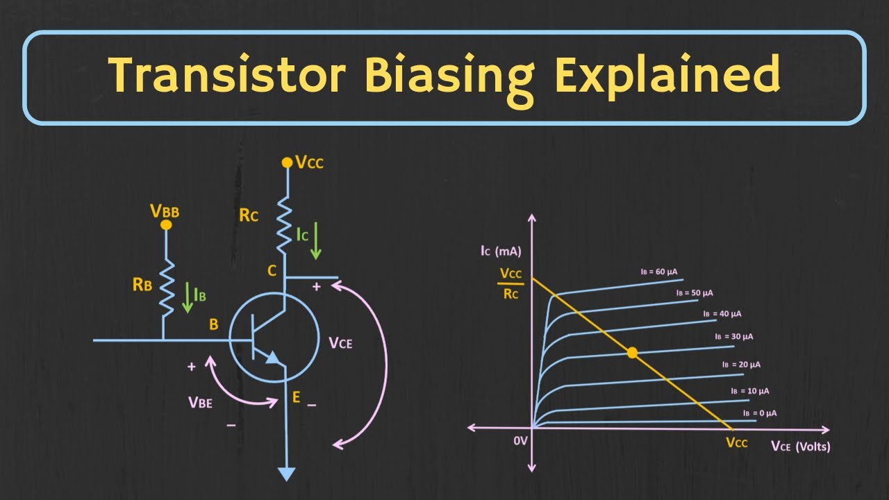
Transistor Biasing: What is Q-point? What is Load Line? Fixed Bias Configuration Explained
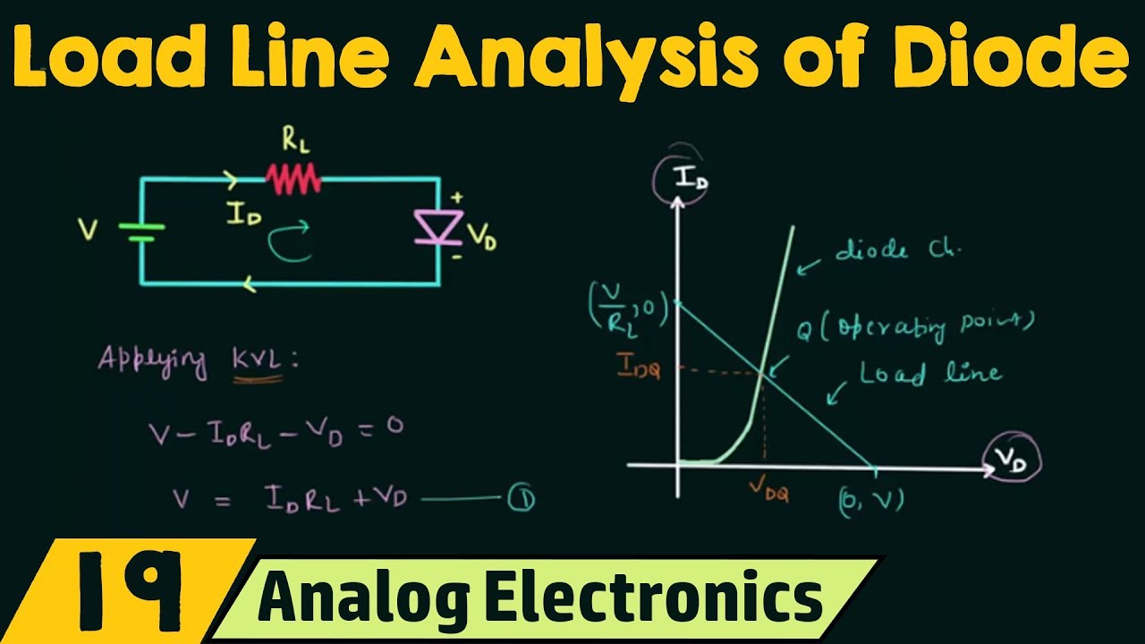
Load Line Analysis of Diode
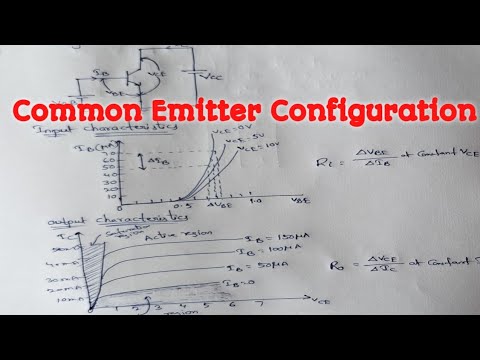
Common Emitter Configuration with input and output characteristics in Telugu//EC&PS//diploma//B.tech
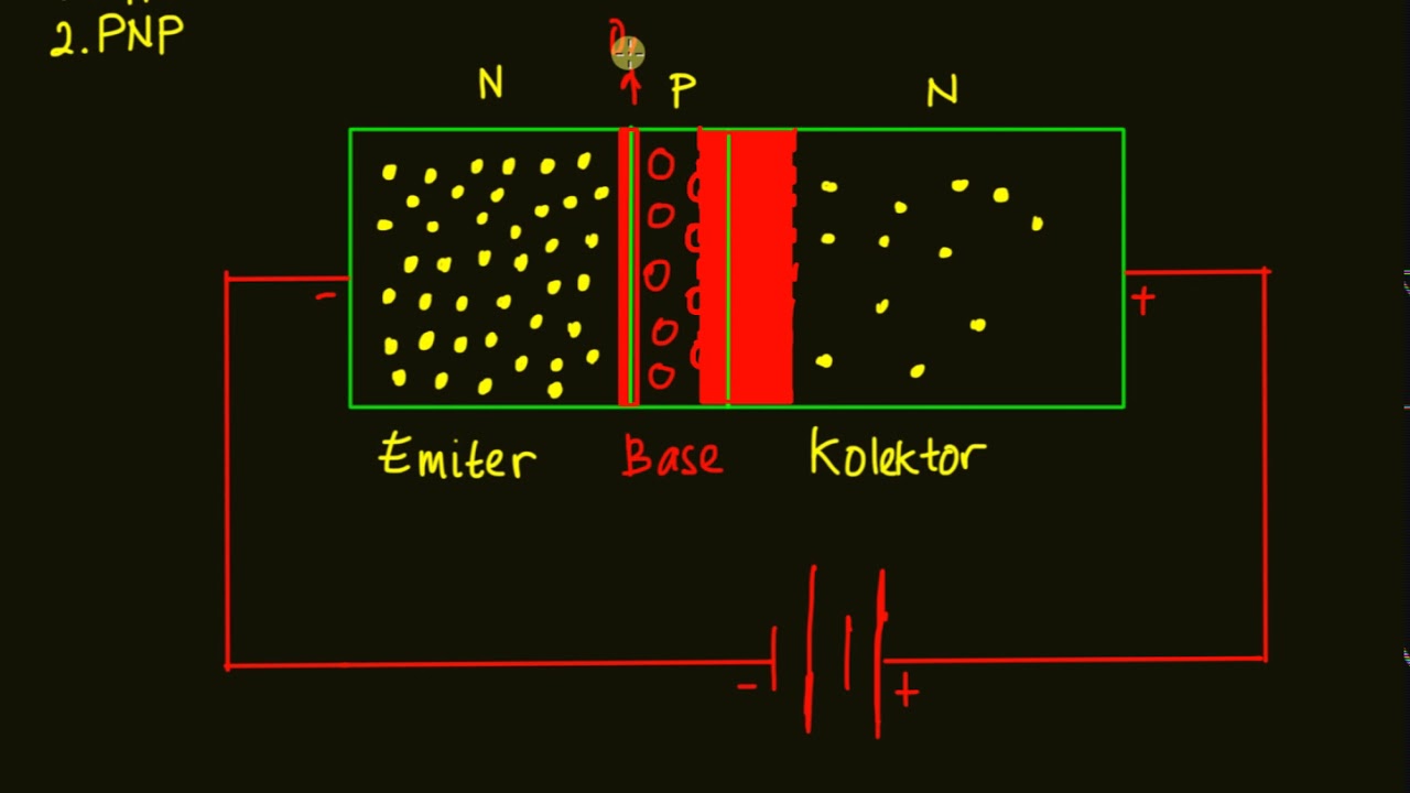
Cara Kerja Bipolar Junction Transistor | Kuliah Fisika Semikonduktor
5.0 / 5 (0 votes)