DC Biasing, Load Line & Operating Point of Transistors
Summary
TLDRThis lecture focuses on biasing of transistors, essential for analyzing their amplifier behavior. It explains the importance of establishing a stable operating point in the active region for faithful signal amplification. The lecture covers the construction of biasing networks, the impact of DC parameters on AC response, and the significance of the input and output operating points. It also discusses how changes in beta values and temperature can affect the operating point, stressing the need for a stable operating point in the center of the active region to prevent signal distortion.
Takeaways
- π Biasing is essential for defining the operating point of a transistor, which is achieved by applying external DC voltages.
- β‘ Transistors have three operating regions: active, saturation, and cutoff. For amplification, the transistor must operate in the active region.
- π Biasing networks are used to maintain the operating point of the transistor in the desired region for proper functioning.
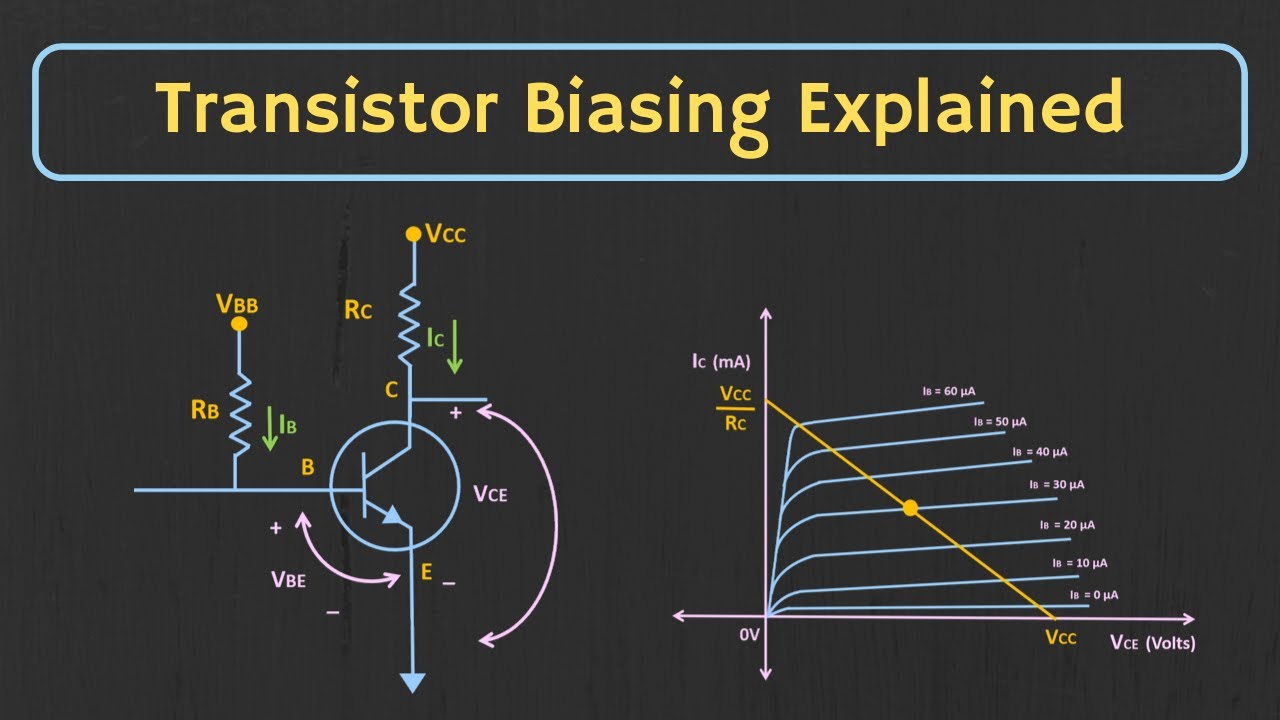
- π§ The common emitter NPN transistor is often used due to its high current amplification capability.
- π Faithful amplification refers to amplifying the input signal without any distortion, which is crucial for ensuring signal integrity.
- π The input operating point is determined by the intersection of the load line with the transistor's input characteristics, based on specific output voltage values.
- π The output operating point is determined by the intersection of the load line with the output characteristics, for a specific base current.
- π¦ Proper placement of the operating point in the middle of the load line prevents distortion, ensuring maximum signal swing.
- π The operating point can shift with changes in resistance or base current, altering the transistor's performance and causing signal distortion.
- π‘οΈ The operating point can also shift due to changes in transistor beta value or temperature, affecting the collector current and leading to potential issues in signal amplification.
Q & A
What is transistor biasing and why is it important?
-Biasing is the process of applying external DC voltages to select the appropriate operating point of a transistor. It is crucial because the operating point determines the transistor's behavior as an amplifier and ensures it operates within the desired region for faithful signal amplification.
What are the three operating regions of a transistor?
-The three operating regions of a transistor are the active region, the saturation region, and the cutoff region. For amplification, the transistor must operate in the active region.
Why is the active region used for amplification in a transistor?
-The active region is used for amplification because, in this region, the transistor can amplify signals without distortion. The transistor operates linearly here, providing a faithful reproduction of the input signal.
What is the function of biasing networks in a transistor circuit?
-Biasing networks are used to establish and maintain the desired operating point of the transistor. They ensure that the transistor remains in the active region for amplification by applying appropriate DC voltages.
What components are involved in a common-emitter NPN transistor circuit?
-In a common-emitter NPN transistor circuit, VBB and VCC are the biasing potentials, RB is the resistance connected in series with the base, and RC is the resistance connected in series with the collector. The emitter is common to both the input and output sides.
How is the input operating point of a transistor determined?
-The input operating point is determined by the intersection of the load line with the transistor's input characteristics for a specific output voltage (VCE). It can be found by applying Kirchhoff's Voltage Law (KVL) in the input loop and plotting the load line based on the input characteristics.
What is the importance of setting the operating point at the center of the active region?
-Setting the operating point at the center of the active region allows for maximum signal swing without distortion. If the operating point is near the cutoff or saturation regions, parts of the amplified signal will be clipped, leading to distortion.
How does changing the base current or collector resistance affect the operating point?
-Increasing the base current shifts the operating point toward higher currents, while decreasing it shifts the operating point toward lower currents. Similarly, increasing the collector resistance changes the slope of the load line, shifting the operating point.
Why does the operating point need to remain stable, and what factors can affect it?
-The operating point needs to remain stable for consistent amplification. It can be affected by changes in the transistorβs beta value (current gain) and temperature variations. Both changes in beta and increased temperature can alter the collector current and shift the operating point.
How does temperature affect the collector current in a transistor?
-Temperature affects the collector current by increasing the leakage current (ICBO), which depends on minority charge carriers. As temperature increases, minority charge carriers and the reverse saturation current increase, causing the collector current to rise and potentially shifting the operating point.
Outlines
π Introduction to Transistor Biasing and Amplification
This paragraph introduces the concept of transistor biasing, explaining that both DC and AC analysis affect each other. Biasing is the process of applying external DC voltages to set the operating point of a transistor, ensuring it functions in the active region for amplification. The paragraph also mentions that the NPN common emitter transistor will be used in the chapter due to its high current amplification capabilities, providing details about the common emitter configuration.
π Understanding Input Operating Point and Load Line
The second paragraph focuses on the input operating point of a transistor, describing how it's determined by the intersection of the load line and the input characteristics curve. It explains the process of plotting the input load line by applying Kirchhoffβs Voltage Law (KVL) in the input loop and calculating key points to determine the load line. The paragraph also covers how changes in output voltage affect the input operating point and how varying the base resistance alters the slope of the load line.
π Output Operating Point and Characteristics Curve
This paragraph dives into the output operating point of a transistor. It explains how the intersection of the load line with the output characteristics for a particular base current defines the output operating point. Similar to the input operating point, the KVL is applied to the output loop to plot the load line. It details how changes in collector resistance (RC) or base current (IB) shift the output operating point, emphasizing that setting the correct operating point is crucial for distortion-free amplification.
π‘ Importance of Setting the Proper Operating Point
This section discusses why it's essential to set the operating point in the middle of the load line, ensuring maximum signal swing without distortion. The paragraph uses examples to illustrate how improper placement of the operating point near the cutoff or saturation regions results in clipping of the output signal. Faithful amplification, with no signal distortion, requires maintaining the operating point in the center of the active region, regardless of changes in temperature or beta variations in transistors.
Mindmap
Keywords
π‘Biasing
π‘DC and AC Analysis
π‘Operating Point
π‘Active Region
π‘NPN Common Emitter
π‘Input and Output Characteristics
π‘Load Line
π‘KVL (Kirchhoff's Voltage Law)
π‘Saturation and Cutoff Regions
π‘Faithful Amplification
Highlights
The analysis of a transistor as an amplifier requires understanding both DC and AC responses, as the parameters chosen in DC analysis affect the AC response and vice versa.
Biasing is the process of applying external DC voltages to select an appropriate operating point for the transistor, and biasing networks are used for this purpose.
A transistor operates in three regions: active, saturation, and cutoff. To use a transistor as an amplifier, it must operate in the active region.
In this chapter, an NPN common emitter transistor is used because of its high current amplification capabilities.
Faithful amplification means amplifying the input signal without distortion, maintaining the shape of the input waveform in the amplified output.
The input operating point is defined as the intersection of the load line with the transistor's input characteristics for a given output voltage (VCE).
To plot the input load line, key points are calculated where VBE = 0 and IB = 0, providing coordinates to draw the load line and find the input operating point.
The output operating point is determined by the intersection of the load line with the transistorβs output characteristics for a given base current (IB).
Setting the proper operating point is crucial to prevent signal distortion. If the operating point is near saturation or cutoff, portions of the waveform will be clipped.
The operating point should be in the center of the active region to allow for maximum signal swing without distortion.
Changes in collector current can shift the operating point, which can occur due to changes in the transistor's beta value or temperature variations.
Beta, the current gain of a transistor, can vary between different transistors, leading to changes in collector current and operating point.
Temperature changes affect the leakage current (ICBO), which is dependent on the minority charge carriers, causing the collector current to increase and potentially shift the operating point.
Once the operating point is set, it should not shift due to variations in collector current, as this would affect signal amplification.
Leakage current increases with temperature, which in turn increases collector current, impacting the stability of the operating point.
Transcripts
from this lecture we will start biasing
of transistors the analysis of
transistor as an amplifier requires the
knowledge of both DC and AC response of
the system we can do DC and AC analysis
of a transistor separately but the
parameters chosen in DC analysis will
affect the AC response and the vice
versa is also true once the desired DC
current and voltage levels are defined
we can construct a network that will
establish the desired operating point so
we have to construct a network to obtain
the desired operating point and for this
purpose we use biasing so what is
biasing biasing is the process in which
we apply external DC voltages to select
in the appropriate operating point this
networks are called as biasing networks
and in this chapter we have to analyze
different types of biasing networks we
already know the three operating regions
of a transistor the first one is the
active region the second one is the
saturation region and the third one is
the cutoff region to use transistor as
an amplifier transistor is biased in
active region this is something we
already know to use transistor as an
amplifier transistor must operate in
active region we already know what is
biasing biasing is the process in which
we apply external DC voltages to select
the appropriate or proper operating
point so we need to bias the transistor
or apply the external DC voltages in a
way so that the operating point of the
transistor remains in active region
throughout our analysis in this chapter
we will use NPN common emitter
transistor we will use n PN common
emitter transistor because of high
current amplification in case of common
emitter transistor
this is the common emitter configuration
using NPN transistor VBB and VCC are the
biasing potentials RB is the resistance
connected in series with the base and RC
is the resistance connected in series
with the collector you can see emitter
is common to the input side and to the
output side the input voltage the input
voltage is vbe the input current is IB
the output voltage the output voltage is
VCE and the output current is IC we want
to amplify the weak input signal
faithfully by faithfully we mean the
amplification of input signal without
any distortion if we apply if we apply
an input signal here then we want the
amplified input signal here without any
distortion for example if the input
signal is sinusoidal if the input signal
is sinusoidal then we want the amplified
output signal to be sinusoidal we don't
want any portion of this waveform to be
clipped this is what we mean by the
faithful amplification of the input
signal the next thing is the operating
point the next thing is the operating
point we are talking about transistors
and transistors are two-port devices so
we have two types of operating points
the first one is the input operating
point and we can define input operating
point as the coordinates obtained by the
intersection of load line with the
transistor input characteristics for the
particular value of output voltage VCE
for this purpose we need to apply the
KVL in the input loop and we also have
to drawn the input characteristics and
then we will draw the load line and the
point of intersection between the load
line and the input characteristics for a
particular output voltage will give us
the input operating point so
we'll quickly I will quickly draw the
input characteristics of the common
emitter transistor we already know how
to draw in the input characteristics of
the common emitter transistor this is
v-b-e
involves and this is IB the base current
in micro amps it is similar to the
forward bias characteristics of PN
Junction diode initially the current is
zero then it increases slowly like this
and once vbe is greater than the barrier
potential the current increases rapidly
like this so this is the input
characteristics of common emitter
transistor and I'm considering silicon
diode because of this the barrier
potential is equal to 0.7 volts now we
will apply the KVL in the input loop so
we have plus vb b plus vb b minus ibrb
drop across this resistance is ib RB so
we have minus ib RB minus vbe minus vbe
equal to 0 and by using this equation we
will draw the load line
in this equation you can see vbe is the
x-axis and IB is the y-axis and to draw
the load line we need two points let's
say first point is p1 and this point is
having x-coordinate equal to 0 and we
have to find out the y coordinate in the
second point point P to the y coordinate
is 0 and we have to find out x
coordinate this means in the first point
in the first point vbe is equal to 0 and
we have to find out value of IB we can
easily calculate the value of IB using
this equation when vbe is equal to 0 ib
is simply equal to vb b divided by RB so
the y-coordinate is equal to VB B
divided by RB for the first point in the
second point y-coordinate is 0 this
means I be the base current is zero and
by using this equation vbe is equal to
VB beam so the x-coordinate is equal to
VB B for the second point and by using
these two points we can easily plot the
load line the first point p1 is having
the coordinates 0 x coordinate is 0 and
the y coordinate is VB B divided by RB
this is point P 1 and this is point P 2
having the coordinates VB be 0 I will
join the two points and the obtained
line is the load line and the point of
intersection is the input operating
point we can easily find out the
coordinates of input operating point the
x coordinate is vbe q the x coordinate
is V
q and the y coordinate the y coordinate
is IBQ the y coordinate is IB Q so these
are the coordinates of input operating
point for particular output voltage VCE
1 if we increase the output voltage the
curve will shift to the right and if we
decrease the output voltage the curve
will shift to the left you can see we
have new operating points this is Q 1
and this operating point is Q 2 we can
also change the operating point by
changing the resistance I'll be slope of
this curve slope of this curve is minus
1 by RB and if we increase our B the
slope will decrease if we increase our B
the slope will decrease and this will be
the new load line and you can see the
operating point is now changed and if
you decrease RB the slope will increase
and the new operating point will shift
to this point so this is all for input
operating point now we will move to the
output operating point in case of output
operating point the intersection of load
line with the transistor output
characteristics for particular value of
base current IB gives the operating
point this is the output characteristics
of common emitter transistor and to find
out the output operating point we need
to draw the load line I will use KVL in
the output loop and we have VCC minus
ICRC minus VCE equal to 0 and by using
this equation we can easily find out
coordinates of two points we need to
repeat the same process as we did in
case of input load line when VCE is
equal to 0 when VCE is equal to 0 the
collector current IC is equal to VCC
divided by RC
and when IC is equal to zero VCE is
equal to VCC now we can easily plot we
can easily plot the load line this point
here is having coordinates equal to zero
VCC by RC and this point here is having
the coordinates equal to VCC zero now I
will join the two points and the
obtained line is the load line and the
point of intersection is the output
operating point I am considering this
intersection point instead of this this
this and this intersection points
because we have to consider the
particular base current and the base
current is IB Q which we have obtained
in the last step the base current was IB
Q so the operating point is this point
and we can easily obtain we can easily
obtain the coordinates of the operating
point the x coordinate is equal to V CEQ
and the y coordinate is equal to IC Q Q
in this symbol represents the operating
point or the qsn point so this is all
you have to do in case of output
operating point and you can clearly see
the operating point will change if we
change the base current if we increase
the base current then the operating
point will shift to this point and if we
decrease the base current the operating
point will shift to this point we can
also change the operating point by
changing the resistance RC the slope the
slope is equal to minus 1 by RC this
slope is negative and if we increase RC
the load line will change and we have a
new load line like this and the
operating point will shift to this point
and if we decrease if we decrease RC the
load line will change because of
increasing
slope and this is the new operating
point setting of proper operating point
is basic thing for amplification of weak
signals I will explain the reason for
this I will explain why setting of
operating point is very important in
this case you can see the operating
point is in the middle is almost in the
middle of the load line and this is
important because if operating point is
near to the saturation region or to the
cutoff region we will not have the
distortion less output signal let's try
to understand this thing in detail I
will paste the output characteristics of
the common emitter transistor
we will analyze two cases in the first
case this is the load line and in the
second case this is the load line let's
say this load line is load line one and
this load line is load line two in case
of first load line the point of
intersection between the load line and
the output characteristics for the
particular base current is q1 and in
this case the operating point is q2 the
value of output voltage at this point is
equal to VCC the supply voltage now we
will plot the output voltage for the two
cases in the first case the amplified
output voltage will have waveform like
this and we already know the output
voltage the output voltage can be equal
to or less than the supply voltage but
here in this case you can see the output
voltage is greater than the supply
voltage VCC so this is not possible and
this portion of the waveform will clip
off and the output voltage is having
Distortion in the same way if we analyze
the second case if we analyze the second
case and plot the output waveform plot
the output waveform you can see you can
see negative portion of the waveform is
clipped why negative portion of the
waveform is clipped because this is the
maximum value of the current and the
waveform cannot have the current more
than this value because of this the
negative portion of the waveform is
clipped and we again have distortion in
the output signal so you can see when
operating point is near to the cutoff
region the positive portion of the
waveform is clipped
and when operating point is near to the
saturation region the negative portion
of the waveform is clipped because of
this the operating point must be
selected in the center of the active
so that we can have the maximum swing
without distortion for example for
example if this is the load line then
this is the operating point let's say it
is Q and in this case if we plot the
amplified output signal and then you can
see then you can see there is no
distortion and we have distortion free
amplified output signal so this is the
faithful amplification of the input
signal and because of this operating
point must remain in the center of the
active region once we set in the proper
operating point it should not shift
because of change in the collector
current once the operating point is
fixed it should not change with change
in the collector current and the
collector current may change because of
two reasons the first reason is change
in beta value is change in beta value we
already know collector current IC is
equal to beta times IB and if beta if
beta increases this implies the
collector current IC will also increase
now how beta increases in case of
transistors beta of two transistors are
different having same beta for two
transistor is very difficult and if we
replace the transistor with other
transistor beta also changes this is
very important point beta value of two
transistors are rarely same the next
thing is change in temperature the next
thing is change in temperature IC the
collector current IC is equal to beta
times IB plus beta plus one I CBO I CBO
is the leakage current and this current
only depends on the minority charge
carriers and the minority charge
carriers only depends on the temperature
if temperature increases minority charge
carriers will increase and also the
leakage current so if temperature
increases this implies the reverse
saturation
current will increase and when reverse
saturation current increases from this
equation you can see the collector
current also increases and from the
characteristics curve you can see if I
see changes the load line will change
and also the operating point this is all
for this lecture see you in the next one
5.0 / 5 (0 votes)