Digital Electronics Ders 1 | MOSFET’e Giriş (İngilizce Terminoloji, Türkçe Anlatım)
Summary
TLDRThis video introduces the fundamentals of digital electronics, focusing on semiconductor devices. It explores the differences between two-terminal devices like diodes and three-terminal devices, such as MOSFETs and BJTs. The video explains how MOSFETs, with their smaller size, lower power consumption, and easier manufacturing, are dominant in integrated circuits. The working principle of MOSFETs is discussed, including the role of gate voltage in creating a conductive channel. The video also touches on MOSFET capacitance and the importance of threshold voltage in controlling current flow, providing insights into the device's structure and operation.
Takeaways
- 😀 MOSFETs (Metal Oxide Semiconductor Field-Effect Transistors) have wide applications in digital electronics, especially in integrated circuits (ICs).
- 😀 Unlike two-terminal semiconductor devices (e.g., diodes), three-terminal semiconductor devices like MOSFETs and BJTs are more versatile and widely used in digital circuits.
- 😀 The key feature of three-terminal semiconductor devices is that a voltage applied to one terminal (gate) controls the current flowing between the other two terminals (source and drain).
- 😀 MOSFETs are preferred over BJTs in IC designs due to their smaller size, lower power consumption, and easier manufacturing process.
- 😀 The structure of a MOSFET includes a P-type substrate, N-type source and drain regions, and a metal gate separated from the channel by an insulator.
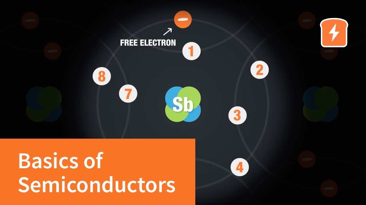
- 😀 Doping in semiconductors (e.g., adding phosphorus to create N-type or boron to create P-type materials) is essential for controlling electrical conductivity.
- 😀 The MOSFET works based on the principle of field-effect, where the gate voltage controls the formation of a conductive channel between the source and drain.
- 😀 When no voltage is applied to the gate, the MOSFET behaves like two back-to-back diodes, blocking current between the source and drain.
- 😀 To turn the MOSFET on, a positive voltage (VGS) is applied to the gate, which attracts electrons and forms a conductive channel in an N-channel MOSFET.
- 😀 The threshold voltage (VT) is the minimum gate voltage required to create a conductive channel in a MOSFET. The conductivity of the channel increases as the gate voltage exceeds the threshold voltage.
- 😀 The capacitance of the MOSFET channel can be calculated based on its dimensions (L and W) and the dielectric material between the gate and the channel. The capacitance plays a role in determining the MOSFET's behavior and efficiency.
Q & A
What is the primary difference between two-terminal and three-terminal semiconductor devices?
-The primary difference is that three-terminal devices, such as transistors, offer a broader range of applications compared to two-terminal devices. Three-terminal devices can amplify signals and control currents, making them more versatile in applications like logic gates and memory elements.
How does a three-terminal semiconductor device function?
-A three-terminal semiconductor device functions by applying a voltage to two terminals, which in turn controls the current at the third terminal. This makes the device act as a controlled current source, similar to how an amplifier works.
Why are MOSFETs preferred over BJTs in digital electronic circuits?
-MOSFETs are preferred over BJTs because they are smaller in size, easier to manufacture, consume less power, and can be used in designs with minimal or no resistance. This makes them more suitable for integrated circuits (ICs), where millions or even billions of MOSFETs are used.
What is the significance of MOSFETs in modern integrated circuits?
-MOSFETs play a crucial role in modern integrated circuits (ICs) due to their small size, low power consumption, and ease of fabrication. They are used in various applications like memory elements and microprocessors, with billions of MOSFETs often found in a single IC.
What is the historical background of MOSFETs?
-MOSFETs were first conceptualized in the early 1960s. After the invention of BJTs in 1947, William Shockley worked on field-effect semiconductor elements in 1952. The MOSFET was officially discovered by Davon KH and Martin Etella in 1960, leading to widespread use in electronics.
What are the main components of a MOSFET?
-A MOSFET consists of a P-type substrate, N-type regions (source and drain), a metal gate, an insulating layer (usually silicon dioxide), and a body terminal. The source and drain regions are heavily doped with N-type impurities, while the gate is made of metal and separated from the substrate by the insulating layer.
What happens when no voltage is applied to the gate of a MOSFET?
-When no voltage is applied to the gate, the MOSFET behaves like two back-to-back PN junctions. This results in no current flowing from the drain to the source because the device is effectively in an 'off' state with very high resistance.
How does applying a positive voltage to the gate of a MOSFET affect its operation?
-Applying a positive voltage to the gate of a MOSFET induces a depletion region by pushing the positive charge carriers (holes) downward. When the gate voltage exceeds a certain threshold (VT), a conductive channel forms between the source and drain, allowing current to flow.
What is the threshold voltage (VT) in a MOSFET?
-The threshold voltage (VT) is the minimum gate voltage required to create a conductive channel between the source and drain. It varies depending on the MOSFET's design but typically ranges from 0.3V to 3V.
What is the significance of the field effect in MOSFETs?
-The field effect in MOSFETs refers to the control of the channel's conductivity by the electric field created by the gate voltage. As the gate voltage increases beyond the threshold, the field effect enhances the channel's conductivity, allowing current to flow from the drain to the source.
Outlines

このセクションは有料ユーザー限定です。 アクセスするには、アップグレードをお願いします。
今すぐアップグレードMindmap

このセクションは有料ユーザー限定です。 アクセスするには、アップグレードをお願いします。
今すぐアップグレードKeywords

このセクションは有料ユーザー限定です。 アクセスするには、アップグレードをお願いします。
今すぐアップグレードHighlights

このセクションは有料ユーザー限定です。 アクセスするには、アップグレードをお願いします。
今すぐアップグレードTranscripts

このセクションは有料ユーザー限定です。 アクセスするには、アップグレードをお願いします。
今すぐアップグレード関連動画をさらに表示

What is Digital Electronics I Basics of Digital Electronics I Introduction to Digital Electronics

Pengantar Semi Konduktor

Classification of Semiconductors (Intrinsic/Extrinsic, P-Type/N-Type)

Part 5.2 #Latches and #FlipFlops #SequentialCircuits in Digital Electronics in Hindi
How do semiconductors work? (with animation) | Intermediate Electronics

VLSI Roadmap | How to Start Career in VLSI? ECE Complete Guidance
5.0 / 5 (0 votes)
