Transistor Introduction (Bipolar Transistors & its Biasing) Basic Electronics
Summary
TLDRThis video provides an introductory lesson on Bipolar Junction Transistors (BJT) in electronics. It covers the construction of NPN and PNP transistors, their working principles, and differences between them. The video explains the structure, doping levels, and terminal connections (emitter, base, and collector) of BJTs. It also delves into how current flows through the transistor based on the biasing of emitter and collector junctions. The session highlights the importance of doping in the emitter for efficient electron emission and discusses the BJT's applications in mobile phones, computers, and other electronics.
Takeaways
- 😀 The topic is an introductory lesson on Bipolar Junction Transistor (BJT), covered under basic electronics (Unit 2).
- 📚 BJTs are discussed in terms of their structure, types, and applications, starting with the NPN and PNP junctions.
- 🔗 A PN junction diode is created when a P-type and N-type semiconductor are connected.
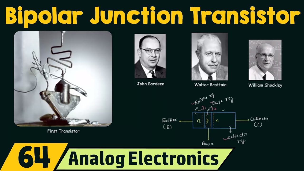
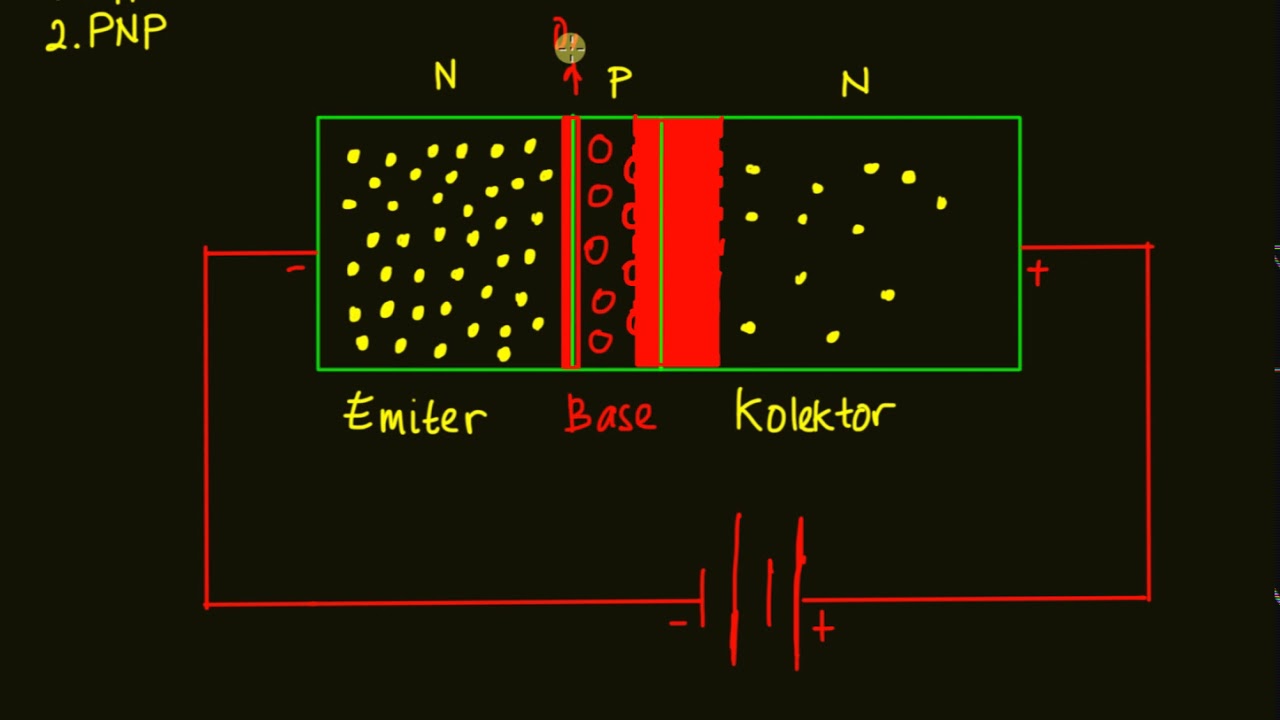
- 💡 Two PN junctions connected form a BJT, which can be NPN or PNP based on their structure.
- 🔍 NPN transistors are more commonly used due to higher electron mobility in N-type semiconductors.
- ⚙️ The three terminals of a transistor are the emitter, base, and collector, with the emitter being heavily doped to release electrons.
- 🔄 The function of the base is to control the flow of electrons, and its size and doping are smaller compared to the emitter.
- ⚡ The collector is the largest part of the transistor and is responsible for collecting electrons from the emitter.
- 🚦 BJTs operate in active mode when the emitter-base junction is forward biased, allowing current to flow.
- 🔧 The symbol of an NPN transistor shows current flowing from base to emitter, and the direction of the arrow indicates electron flow.
Q & A
What is the main topic covered in the video?
-The video covers the basics of Bipolar Junction Transistors (BJTs), specifically focusing on their construction, types, and applications.
What is a Bipolar Junction Transistor (BJT)?
-A Bipolar Junction Transistor (BJT) is a semiconductor device that consists of two PN junctions. It is widely used in electronics for amplification and switching purposes.
What are the two main types of BJTs?
-The two main types of BJTs are NPN and PNP transistors. These differ in the arrangement of their P-type and N-type semiconductor materials.
How is an NPN transistor constructed?
-An NPN transistor is constructed by sandwiching a P-type semiconductor between two N-type semiconductors, forming two PN junctions.
Why is the NPN transistor more commonly used than the PNP transistor?
-The NPN transistor is more commonly used because the mobility of electrons (majority charge carriers in N-type semiconductors) is higher than that of holes (majority carriers in P-type semiconductors), leading to better performance in terms of current flow.
What is the function of the emitter in a BJT?
-The emitter's function is to inject charge carriers (electrons in NPN, holes in PNP) into the base region of the transistor.
What is the importance of doping in BJTs?
-Doping in BJTs is important to control the concentration of charge carriers. The emitter is heavily doped to ensure a high number of charge carriers, while the base is lightly doped and thin to allow efficient charge flow to the collector.
What is the role of the collector in a BJT?
-The collector's role is to collect charge carriers (electrons or holes) from the base. It is larger in size and moderately doped to handle a higher current load.
What does it mean when the emitter-base junction is forward biased?
-When the emitter-base junction is forward biased, the potential barrier is reduced, allowing charge carriers to flow from the emitter into the base, which initiates the transistor's active operation.
How does the base-collector junction operate in reverse bias?
-In reverse bias, the base-collector junction prevents current from flowing directly between the collector and base, allowing the transistor to control current flow between the collector and emitter efficiently.
Outlines

このセクションは有料ユーザー限定です。 アクセスするには、アップグレードをお願いします。
今すぐアップグレードMindmap

このセクションは有料ユーザー限定です。 アクセスするには、アップグレードをお願いします。
今すぐアップグレードKeywords

このセクションは有料ユーザー限定です。 アクセスするには、アップグレードをお願いします。
今すぐアップグレードHighlights

このセクションは有料ユーザー限定です。 アクセスするには、アップグレードをお願いします。
今すぐアップグレードTranscripts

このセクションは有料ユーザー限定です。 アクセスするには、アップグレードをお願いします。
今すぐアップグレード5.0 / 5 (0 votes)


