Construction & Working of Enhancement-Type MOSFET (Part 1)
Summary
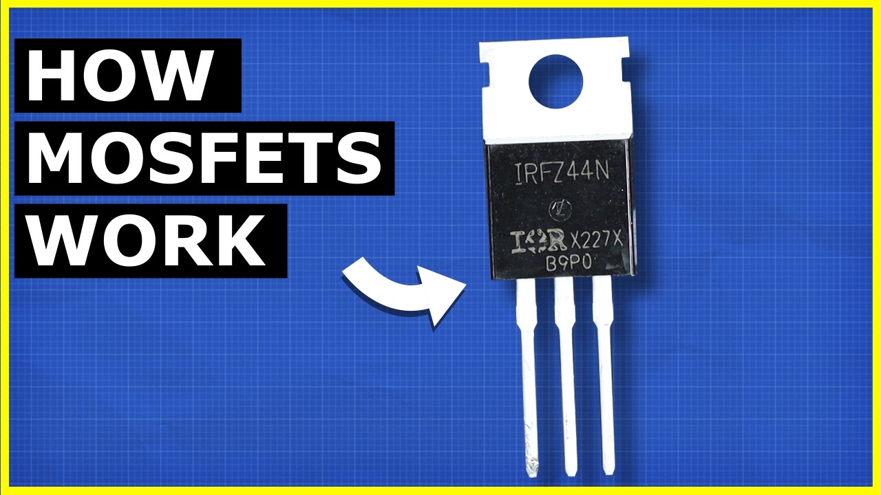
TLDRThis script introduces Metal Oxide Semiconductor Field Effect Transistors (MOSFETs), emphasizing their classification into depletion and enhancement types. It focuses on the n-channel enhancement type MOSFET, detailing its construction and the process of channel formation through inversion, where a positive gate voltage induces a conductive n-type channel between the source and drain in a p-type substrate.
Takeaways
- 😀 An active device is a circuit component capable of controlling the flow of electrons, such as BJT, JFET, and MOSFET.
- 🔋 MOSFETs are classified into two types: depletion type and enhancement type, each with n-channel and p-channel variations.
- 🌐 The construction of depletion and enhancement type MOSFETs is similar, but a key difference is the initial presence of a channel in depletion type MOSFETs.
- 🌐 In an n-channel enhancement type MOSFET, the substrate is p-type, and the source and drain are n-type, while in a p-channel enhancement type MOSFET, the substrate is n-type, and the source and drain are p-type.
- 🔌 The gate terminal of a MOSFET is not in direct contact with the body; it is separated by a thin layer of silicon dioxide, known as the gate oxide.
- 🔬 The gate oxide layer is made very thin (approximately 1,000 angstroms) to allow the gate electrode to control the surface of the semiconductor.
- 🔋 The formation of a channel in an enhancement type MOSFET occurs when the gate terminal is made more positive with respect to the substrate, causing an inversion from p-type to n-type material near the surface.
- 🔄 The process of channel formation is called inversion, where the region near the surface changes from p-type to n-type due to the accumulation of negative charges.
- 🌐 When the gate voltage (Vgs) is increased, the channel width or depth increases, allowing more current to flow between the source and drain.
- 🔬 The lecture will continue to explore the complete working of the n-channel enhancement type MOSFET in the next session.
Q & A
What is an active device in electronics?
-An active device is any type of circuit component with the ability to control the flow of electrons and eventually the current flow.
How does a MOSFET differ from a passive device?
-A MOSFET is an active device because it can control the flow of electrons, unlike passive devices which cannot control the flow of electrons.
What are the two types of MOSFETs?
-The two types of MOSFETs are depletion type MOSFET and enhancement type MOSFET.
What is the main difference between depletion type and enhancement type MOSFETs?
-The main difference is that in a depletion type MOSFET, a channel exists between the drain and source from the beginning, while in an enhancement type MOSFET, there is no channel initially.
What is the purpose of doping the parent material with trivalent impurities in an n-channel enhancement type MOSFET?
-Doping the parent material with trivalent impurities converts it into a P-type material, which is necessary for the construction of an n-channel enhancement type MOSFET.
What are the two end type wells created in the process of constructing an n-channel enhancement type MOSFET?
-The two end type wells created are n-type wells, which act as the source and drain of the MOSFET.
What is the function of the gate terminal in an n-channel enhancement type MOSFET?
-The gate terminal in an n-channel enhancement type MOSFET is not in direct contact with the body. It is located over a thin layer of silicon dioxide and is used to control the channel formation between the source and drain.
Why is the silicon dioxide layer in a MOSFET made very thin?
-The silicon dioxide layer is made very thin to allow for better control over the surface by the gate electrode.
What is the process called when the region near the surface of a P-type material becomes N-type due to the application of a positive voltage to the gate?
-The process is called inversion, where the P-type material is inverted to N-type, creating a conductive channel between the source and drain.
How does increasing the voltage (Vgs) between the gate and substrate terminals affect the channel in an n-channel enhancement type MOSFET?
-Increasing Vgs causes more negative charge to accumulate near the surface, leading to the formation of an n-type channel between the source and drain, thus increasing the channel width or depth.
Outlines

このセクションは有料ユーザー限定です。 アクセスするには、アップグレードをお願いします。
今すぐアップグレードMindmap

このセクションは有料ユーザー限定です。 アクセスするには、アップグレードをお願いします。
今すぐアップグレードKeywords

このセクションは有料ユーザー限定です。 アクセスするには、アップグレードをお願いします。
今すぐアップグレードHighlights

このセクションは有料ユーザー限定です。 アクセスするには、アップグレードをお願いします。
今すぐアップグレードTranscripts

このセクションは有料ユーザー限定です。 アクセスするには、アップグレードをお願いします。
今すぐアップグレード


5.0 / 5 (0 votes)
