TSMC 5nm, 3nm and 2nm devices explained | Technology Node | VLSI | Why such naming? | TSMC
Summary
TLDRIn this video, Jason Jain explains the concept of semiconductor technology nodes, debunking the myth that they represent the physical dimensions of transistors. He highlights how modern nodes, such as 5nm or 3nm, are more about performance improvements like lower power, delay, and area rather than actual transistor sizes. The video delves into the history of transistor development, the transition from planar to 3D FinFETs and GAA architectures, and the marketing implications behind the naming of tech nodes. Ultimately, the video sheds light on how semiconductor companies use these nodes to market and scale their products, focusing on performance rather than size.
Takeaways
- 😀 The term 'technology node' in semiconductor manufacturing doesn't directly refer to the physical dimension of a transistor, such as its gate length or channel length.
- 😀 The 'nanometer' designation in chip manufacturing is more of a marketing number, reflecting performance improvements rather than actual physical size.
- 😀 Transistors have evolved significantly since the 1947 invention, with advances from 1 cm nodes to the current 5 nm and even 1 nm and smaller nodes in development.
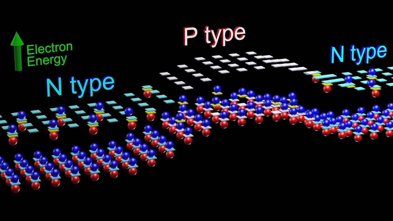
- 😀 The shift from planar CMOS devices to 3D FinFETs and then to Gate-All-Around (GAA) FETs marked a critical change in semiconductor architecture, making the node number less tied to physical dimensions.
- 😀 Companies like Samsung and TSMC are at the forefront of scaling down technology nodes, with Samsung's 3 nm GAA technology already being implemented in mobile phones.
- 😀 The performance of transistors at smaller nodes is characterized by better power efficiency, lower delay, and smaller area, rather than just reduced physical size.
- 😀 Different semiconductor companies define their technology nodes differently, which means that a '5 nm' node from one company may not be equivalent to a '5 nm' node from another.
- 😀 Intel’s marketing has shifted from using traditional technology node names to more abstract ones like 'Intel 7' and 'Intel 4', showcasing how marketing plays a significant role in semiconductor node naming.
- 😀 Semiconductor nodes like 10 nm and 7 nm are not always comparable across different manufacturers—Intel’s 10 nm node, for example, is closer in performance to TSMC’s 7 nm node.
- 😀 Moving to smaller nodes can be extremely expensive, requiring entirely new manufacturing machinery, which can cost millions of dollars to implement.
- 😀 While shrinking technology nodes leads to better-performing chips and higher transistor density, the cost of adoption for these smaller nodes is substantial, making it a challenge for companies to keep up with the pace of innovation.
Q & A
What does the term 'technology node' refer to in semiconductor manufacturing?
-In semiconductor manufacturing, the term 'technology node' refers to the naming convention used to represent the performance of a chip, such as lower delay, lower power consumption, and smaller area. It is not related to the physical dimension of the transistor, but more about the efficiency and performance characteristics of the transistor at that scale.
Why does the technology node number not correspond to the physical size of the transistor anymore?
-The technology node number no longer corresponds to the physical size of the transistor because semiconductor manufacturing has evolved to use more advanced architectures, such as 3D FinFETs and Gate-All-Around (GAA) FETs, which don't directly correlate with the traditional gate length or channel size.
What was the significance of the transition from planar CMOS to 3D FinFET transistors?
-The transition from planar CMOS to 3D FinFET transistors marked a shift in transistor architecture, allowing for better performance by improving power efficiency, speed, and density. This change also led to the technology node number losing its direct relationship to the physical dimensions of the transistor.
What is the role of marketing in semiconductor technology node naming?
-Marketing plays a significant role in semiconductor technology node naming. Companies use technology node names, such as 5nm or 7nm, to attract consumer attention and convey the improved performance and efficiency of their chips. However, these names are primarily used as marketing tools and may not represent the actual physical size of the transistors.
How has Intel adjusted its technology node naming strategy?
-Intel has adjusted its technology node naming strategy by renaming its traditional node names to more appealing, dimensionless labels. For example, Intel’s 10nm process was renamed to 'Intel 7,' and their 7nm process was renamed to 'Intel 4,' in order to better market these technologies and differentiate them in the industry.
How do different semiconductor companies compare their technology nodes?
-Different semiconductor companies, such as Intel, TSMC, and Samsung, often use their own definitions and performance benchmarks for technology nodes. For instance, Intel's 10nm technology is close to TSMC's 7nm and Samsung's 7nm, but the naming conventions differ, and the node numbers may not correspond directly to one another.
Why do companies like TSMC and Samsung push to scale down technology nodes?
-Companies like TSMC and Samsung push to scale down technology nodes in order to improve the performance of their chips, offering better power efficiency, higher processing speeds, and reduced sizes, which are crucial for the advancement of mobile devices, computers, and other tech products.
What new transistor architecture did Samsung and IBM introduce recently?
-Samsung and IBM recently introduced the Gate-All-Around (GAA) transistor architecture, which is an advanced technology used in their 3nm process nodes. This new architecture is designed to improve the performance of transistors by providing better control over the flow of electricity.
How do technology node advancements affect semiconductor manufacturing costs?
-Advancing to a new technology node is costly because it requires the replacement of old machinery with new parametric machines, which can cost millions of dollars. These investments are essential to achieving better chip performance and scalability, but they come at a significant financial expense.
What is the relationship between technology node scaling and the overall profitability of semiconductor companies?
-The scaling down of technology nodes and the resulting improvements in chip performance allow semiconductor companies to offer more powerful and efficient products. This leads to greater market demand and higher sales, thus increasing the profitability of these companies as they continue to innovate and deliver more competitive products.
Outlines

Dieser Bereich ist nur für Premium-Benutzer verfügbar. Bitte führen Sie ein Upgrade durch, um auf diesen Abschnitt zuzugreifen.
Upgrade durchführenMindmap

Dieser Bereich ist nur für Premium-Benutzer verfügbar. Bitte führen Sie ein Upgrade durch, um auf diesen Abschnitt zuzugreifen.
Upgrade durchführenKeywords

Dieser Bereich ist nur für Premium-Benutzer verfügbar. Bitte führen Sie ein Upgrade durch, um auf diesen Abschnitt zuzugreifen.
Upgrade durchführenHighlights

Dieser Bereich ist nur für Premium-Benutzer verfügbar. Bitte führen Sie ein Upgrade durch, um auf diesen Abschnitt zuzugreifen.
Upgrade durchführenTranscripts

Dieser Bereich ist nur für Premium-Benutzer verfügbar. Bitte führen Sie ein Upgrade durch, um auf diesen Abschnitt zuzugreifen.
Upgrade durchführenWeitere ähnliche Videos ansehen
Semiconductors - Physics inside Transistors and Diodes

What is a Transistor | Working Principles
How are Microchips Made? 🖥️🛠️ CPU Manufacturing Process Steps

Introduction to semiconductors

Transistors, How do they work?

Transistor hoạt động như thế nào? | Transistor là gì? | Bóng bán dẫn là gì? | Tri thức nhân loại
5.0 / 5 (0 votes)
