Integrated Circuits & Moore's Law: Crash Course Computer Science #17
Summary
TLDRThis CrashCourse Computer Science episode explores the evolution of computing hardware, from the complexity of early machines like ENIAC to the advent of integrated circuits (ICs) by Jack Kilby and Robert Noyce. It explains how ICs, along with printed circuit boards (PCBs), revolutionized electronics, leading to Moore's Law and the exponential growth in transistor density. The episode also touches on the current challenges in miniaturization and the future of computing.
Takeaways
- đĄ The evolution of software from machine code to object-oriented programming was enabled by advancements in hardware.
- đ The growth in computing power was initially limited by the complexity of discrete components, known as the 'Tyranny of Numbers'.
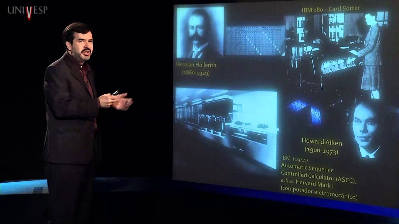
- đ Transistors replaced vacuum tubes in the mid-1950s, leading to the second generation of electronic computing and addressing some of the limitations of vacuum tubes.
- đïž Integrated Circuits (ICs), introduced in the late 1950s, revolutionized computer design by integrating multiple components into a single unit.
- đ Robert Noyce is credited as the father of modern ICs, using silicon as the base material, which led to the rise of Silicon Valley.
- đ Printed Circuit Boards (PCBs) simplified the manufacturing process by allowing metal wires to be etched directly onto a board, reducing the need for manual soldering.
- đŹ Photolithography was a pivotal fabrication process that enabled the creation of complex circuits on a single piece of silicon, leading to higher density and performance.
- đ Moore's Law, observed in 1965, predicted the doubling of transistors on a chip approximately every two years, which has largely held true for decades.
- đ The cost of ICs decreased dramatically over time, making them more accessible and leading to widespread adoption in electronics.
- đ The Intel 4004, released in 1971, was a milestone as the first microprocessor, showcasing the potential of integrated circuits in compact computing.
- đ While Moore's Law may be nearing its limits due to physical constraints, ongoing research into new materials and processes could extend the trend.
Q & A
What was the 'Tyranny of Numbers' in the context of early computer hardware?
-The 'Tyranny of Numbers' referred to the increasing complexity and unwieldiness of designing and manufacturing computers with hundreds of thousands of individual components, each requiring connections and wires, as performance demands grew.
How did the advent of transistors impact the development of computers?
-Transistors, which became commercially available in the mid-1950s, were smaller, faster, and more reliable than vacuum tubes. They marked the second generation of electronic computing, leading to computers that were faster and more cost-effective.
What was the significance of Jack Kilby's demonstration at Texas Instruments in 1958?
-Jack Kilby demonstrated an electronic part where all components of an electronic circuit were integrated into a single unit, which was the first step towards the development of Integrated Circuits (ICs).
Why is Robert Noyce considered the father of modern ICs?
-Robert Noyce, working at Fairchild Semiconductor, made ICs practical by using abundant and stable silicon instead of the rare and unstable germanium used by Jack Kilby, thus ushering in the electronics era and contributing to the rise of Silicon Valley.
How did the use of Printed Circuit Boards (PCBs) revolutionize computer manufacturing?
-PCBs allowed for the mass manufacturing of boards with metal wires etched directly into them to connect components, reducing the need for manual soldering and bundling of countless wires, which made computers smaller, cheaper, and more reliable.
What is Photolithography and how is it used in the production of ICs?
-Photolithography is a process that uses light to transfer complex patterns onto a material like a semiconductor. It involves several steps including applying a photoresist, using a photomask, and etching to create the desired pattern, which is fundamental in building transistors and other electronic components on a silicon wafer.
What is Moore's Law and how has it influenced the development of ICs?
-Moore's Law is the observation made by Gordon Moore in 1965 that the number of transistors on a chip doubles approximately every two years. This trend has driven the continuous miniaturization and increase in performance of ICs.
How did the Intel 4004 CPU represent a significant milestone in computing?
-The Intel 4004, released in 1971, was the first microprocessor to be shipped as an IC, containing 2,300 transistors. It symbolized the shift to the third generation of computing, where entire CPUs could be integrated into a single chip.
What are the two main challenges facing further miniaturization of transistors?
-The two main challenges are the physical limits of how fine features can be made on a photomask due to the wavelengths of light used in photolithography, and quantum tunneling, where electrons can jump the gap between electrodes when transistors are made extremely small.
How has the development of VLSI software impacted the design of ICs?
-VLSI (Very-Large-Scale Integration) software has automated the process of chip design, using techniques like logic synthesis to efficiently lay out high-level components, which has been crucial as the complexity of ICs has grown exponentially.
Outlines
đ» The Evolution of Computing Hardware
This segment of the video script delves into the history and evolution of computer hardware. It starts by highlighting the transition from early programming efforts to modern software engineering practices, emphasizing the role of hardware improvements in this growth. The discussion then takes a trip back to the birth of electronic computing, detailing the shift from discrete components to integrated circuits. The ENIAC's construction with thousands of vacuum tubes and the advent of transistors are mentioned, illustrating the move towards smaller, faster, and more reliable components. The segment also covers the development of printed circuit boards and the significance of Jack Kilby's and Robert Noyce's work in creating integrated circuits, which paved the way for Silicon Valley and the modern electronics era.
đŹ The Process of Photolithography in IC Fabrication
Paragraph 2 focuses on the intricate process of photolithography, which revolutionized the manufacturing of integrated circuits (ICs). It describes the steps involved in creating an IC, starting from a silicon wafer and adding protective oxide layers. The script explains how photoresist is applied and selectively removed using a photomask and light exposure, allowing for the precise etching of the oxide layer to form transistors. The importance of doping to alter the silicon's electrical properties is also covered. The segment further details the multiple rounds of photolithography required to build a transistor and the subsequent steps to create metal channels for wiring. It concludes with a look at how ICs have evolved over time, with Moore's Law highlighting the trend of increasing transistor density and the subsequent benefits in terms of speed, power consumption, and cost.
đ The Impact of Integrated Circuits on Modern Computing
The final paragraph of the script discusses the impact of integrated circuits on the computing industry, marking the transition to the third generation of computing. It marvels at the integration levels achieved, exemplified by the Intel 4004 microprocessor. The script outlines the exponential growth in CPU transistor counts over the decades, leading to the development of increasingly powerful and compact processors. It touches on the advancements in photolithography that have enabled these improvements, as well as the challenges faced in further miniaturization due to the limitations of light wavelengths and quantum tunneling. The segment also mentions the role of VLSI software in automating chip design and the potential future of transistor technology, hinting at ongoing research into even smaller, 1-nanometer transistors.
Mindmap
Keywords
đĄDiscrete Components
đĄTransistors
đĄIntegrated Circuits (ICs)
đĄPrinted Circuit Boards (PCBs)
đĄPhotolithography
đĄDoping
đĄMoore's Law
đĄMicroprocessor
đĄVery-Large-Scale Integration (VLSI)
đĄQuantum Tunneling
Highlights
The evolution of software complexity from machine code to object-oriented programming was enabled by hardware improvements.
Early computers like ENIAC used thousands of vacuum tubes and required millions of soldered connections.
The transition from vacuum tubes to transistors in the 1950s marked the second generation of electronic computing.
IBM's 7090, a transistorized computer, was six times faster and half the cost of its vacuum-tube-based predecessor.
The 'Tyranny of Numbers' problem highlighted the need for a new level of abstraction in computer design.
Jack Kilby's demonstration of an integrated circuit at Texas Instruments in 1958 was a breakthrough in electronics.
Robert Noyce's use of silicon made integrated circuits more practical and reliable, earning him the title 'father of modern ICs'.
Integrated Circuits (ICs) allowed for the miniaturization and increased reliability of computer components.
Printed Circuit Boards (PCBs) revolutionized manufacturing by allowing for the mass production of interconnected components.
Photolithography enabled the creation of complex circuits by using light to transfer patterns onto semiconductors.
The Intel 4004, released in 1971, was the first microprocessor and a significant milestone in computing.
Moore's Law, observed in 1965, predicted the doubling of transistors in ICs every two years, a trend that held for decades.
The cost of ICs dramatically decreased from $50 in 1962 to around $2 in 1968, making technology more accessible.
Smaller transistors led to faster switching speeds, less power consumption, and higher clock speeds in CPUs.
Intel, founded by Robert Noyce and Gordon Moore, became the largest chip maker, leading the microprocessor revolution.
Modern CPUs like the A10 in the iPhone 7 contain billions of transistors, showcasing the exponential growth in IC density.
VLSI software has automated chip design, marking the beginning of the fourth generation of computers.
The end of Moore's Law is predicted due to physical limits in photolithography and quantum tunneling effects.
Despite challenges, researchers are exploring solutions like smaller light wavelengths and 1-nanometer transistors.
Transcripts
This episode is brought to you by Curiosity Stream.
Hi, Iâm Carrie Anne, and welcome to CrashCourse Computer Science!
Over the past six episodes, we delved into software, from early programming efforts to
modern software engineering practices.
Within about 50 years, software grew in complexity from machine code punched by hand onto paper
tape, to object oriented programming languages, compiled in integrated development environments.
But this growth in sophistication would not have been possible without improvements in hardware.
INTRO
To appreciate computing hardwareâs explosive growth in power and sophistication, we need
to go back to the birth of electronic computing.
From roughly the 1940âs through the mid-1960s, every computer was built from individual parts,
called discrete components, which were all wired together.
For example, the ENIAC, consisted of more than 17,000 vacuum tubes, 70,000 resistors,
10,000 capacitors, and 7,000 diodes, all of which required 5 million hand-soldered connections.
Adding more components to increase performance meant more connections, more wires, and just
more complexity, what was dubbed the Tyranny of Numbers.
By the mid 1950s, transistors were becoming commercially available and being incorporated
into computers.
These were much smaller, faster and more reliable than vacuum tubes, but each transistor was
still one discrete component.
In 1959, IBM upgraded their vacuum-tube-based â709â computers to transistors by replacing
all the discrete vacuum tubes with discrete transistors.
The new machine, the IBM 7090, was six times faster and half the cost.
These transistorized computers marked the second generation of electronic computing.
However, although faster and smaller, discrete transistors didnât solve the Tyranny of
Numbers.
It was getting unwieldy to design, let alone physically manufacture computers with hundreds
of thousands of individual components.
By the the 1960s, this was reaching a breaking point.
The insides of computers were often just huge tangles of wires.
Just look at what the inside of a PDP-8 from 1965 looked like!
The answer was to bump up a new level of abstraction, and package up underlying complexity!
The breakthrough came in 1958, when Jack Kilby, working at Texas Instruments, demonstrated
such an electronic part, âwherein all the components of the electronic circuit are completely
integrated."
Put simply: instead of building computer parts out of many discrete components and wiring
them all together, you put many components together, inside of a new, single component.
These are called Integrated Circuits, or ICs.
A few months later in 1959, Fairchild Semiconductor, lead by Robert Noyce, made ICs practical.
Kilby built his ICs out of germanium, a rare and unstable material.
But, Fairchild used the abundant silicon, which makes up about a quarter of the earth's crust!
Itâs also more stable, therefore more reliable.
For this reason, Noyce is widely regarded as the father of modern ICs, ushering in the
electronics era... and also Silicon Valley, where Fairchild was based and where many other
semiconductor companies would soon pop up.
In the early days, an IC might only contain a simple circuit with just a few transistors,
like this early Westinghouse example.
But even this allowed simple circuits, like the logic gates from Episode 3, to be packaged
up into a single component.
ICs are sort of like lego for computer engineers âbuilding blocksâ that can be arranged
into an infinite array of possible designs.
However, they still have to be wired together at some point to create even bigger and more
complex circuits, like a whole computer.
For this, engineers had another innovation: printed circuit boards, or PCBs.
Instead of soldering and bundling up bazillions of wires, PCBs, which could be mass manufactured,
have all the metal wires etched right into them* to connect components together.
By using PCBs and ICs together, one could achieve exactly the same functional circuit
as that made from discrete components, but with far fewer individual components and tangled
wires.
Plus, itâs smaller, cheaper and more reliable.
Triple win!
Many early ICs were manufactured using teeny tiny discrete components packaged up as a
single unit, like this IBM example from 1964.
However, even when using really really itty-bitty components, it was hard to get much more than
around five transistors onto a single IC.
To achieve more complex designs, a radically different fabrication process was needed that
changed everything: Photolithography!
In short, itâs a way to use light to transfer complex patterns to a material, like a semiconductor.
It only has a few basic operations, but these can be used to create incredibly complex circuits.
Letâs walk through a simple, although extensive example, to make one of these!
We start with a slice of silicon, which, like a thin cookie, is called a wafer.
Delicious!
Silicon, as we discussed briefly in episode 2, is special because itâs a semiconductor,
that is, a material that can sometimes conduct electricity and other times does not.
We can control where and when this happens, making Silicon the perfect raw material for
making transistors.
We can also use a wafer as a base to lay down complex metal circuits, so everything is integrated,
perfect for... integrated circuits!
The next step is to add a thin oxide layer on top of the silicon, which acts as a protective
coating.
Then, we apply a special chemical called a photoresist.
When exposed to light, the chemical changes, and becomes soluble, so it can be washed away
with a different special chemical.
Photoresists arenât very useful by themselves, but are super powerful when used in conjunction
with a photomask.
This is just like a piece of photographic film, but instead of a photo of a hamster
eating a tiny burrito, it contains a pattern to be transferred onto the wafer.
We do this by putting a photomask over the wafer, and turning on a powerful light.
Where the mask blocks the light, the photoresist is unchanged.
But where the light does hit the photoresist it changes chemically which lets us wash away
only the photoresist that was exposed to light, selectively revealing areas of our oxide layer.
Now, by using another special chemical, often an acid, we can remove any exposed oxide,
and etch a little hole the entire way down to the raw silicon.
Note that the oxide layer under the photoresist is protected.
To clean up, we use yet another special chemical that washes away any remaining photoresist.
Yep, there are a lot of special chemicals in photolithography, each with a very specific
function!
So now we can see the silicon again, we want to modify only the exposed areas to better
conduct electricity.
To do that, we need to change it chemically through a process called: doping.
Iâm not even going to make a joke.
Letâs move on.
Most often this is done with a high temperature gas, something like Phosphorus, which penetrates
into the exposed area of silicon.
This alters its electrical properties.
Weâre not going to wade into the physics and chemistry of semiconductors, but if youâre
interested, thereâs a link in the description to an excellent video by our friend Derek
Muller from Veritasium.
But, we still need a few more rounds of photolithography to build a transistor.
The process essentially starts again, first by building up a fresh oxide layer ...which
we coat in photoresist.
Now, we use a photomask with a new and different pattern, allowing us to open a small window
above the doped area.
Once again, we wash away remaining photoresist.
Now we dope, and avoid telling a hilarious joke, again, but with a different gas that
converts part of the silicon into yet a different form.
Timing is super important in photolithography in order to control things like doping diffusion
and etch depth.
In this case, we only want to dope a little region nested inside the other.
Now we have all the pieces we need to create our transistor!
The final step is to make channels in the oxide layer so that we can run little metal
wires to different parts of our transistor.
Once more, we apply a photoresist, and use a new photomask to etch little channels.
Now, we use a new process, called metalization, that allows us to deposit a thin layer of
metal, like aluminium or copper.
But we donât want to cover everything in metal.
We want to etch a very specific circuit design.
So, very similar to before, we apply a photoresist, use a photomask, dissolve the exposed resist,
and use a chemical to remove any exposed metal.
Whew!
Our transistor is finally complete!
It has three little wires that connect to three different parts of the silicon, each
doped a particular way to create, in this example, whatâs called a bipolar junction transistor.
Hereâs the actual patent from 1962, an invention that changed our world forever!
Using similar steps, photolithography can create other useful electronic elements, like
resistors and capacitors, all on a single piece of silicon (plus all the wires needed
to hook them up into circuits).
Goodbye discrete components!
In our example, we made one transistor, but in the real world, photomasks lay down millions
of little details all at once.
Here is what an IC might look like from above, with wires crisscrossing above and below each
other, interconnecting all the individual elements together into complex circuits.
Although we could create a photomask for an entire wafer, we can take advantage of the
fact that light can be focused and projected to any size we want.
In the same way that a film can be projected to fill an entire movie screen, we can focus
a photomask onto a very small patch of silicon, creating incredibly fine details.
A single silicon wafer is generally used to create dozens of ICs.
Then, once youâve got a whole wafer full, you cut them up and package them into microchips,
those little black rectangles you see in electronics all the time.
Just remember: at the heart of each of those chips is one of these small pieces of silicon.
As photolithography techniques improved, the size of transistors shrunk, allowing for greater
densities.
At the start of the 1960s, an IC rarely contained more than 5 transistors, they just couldnât
possibly fit.
But, by the mid 1960s, we were starting to see ICs with over 100 transistors on the market.
In 1965, Gordon Moore could see the trend: that approximately every two years, thanks
to advances in materials and manufacturing, you could fit twice the number of transistors
into the same amount of space.
This is called Mooreâs Law.
The term is a bit of a misnomer though.
Itâs not really a law at all, more of a trend.
But itâs a good one.
IC prices also fell dramatically, from an average of $50 in 1962 to around $2 in 1968.
Today, you can buy ICs for cents.
Smaller transistors and higher densities had other benefits too.
The smaller the transistor, the less charge you have to move around, allowing it to switch
states faster and consume less power.
Plus, more compact circuits meant less delay in signals resulting in faster clock speeds.
In 1968, Robert Noyce and Gordon Moore teamed up and founded a new company, combining the
words Integrated and Electronics...
Intel... the largest chip maker today.
The Intel 4004 CPU, from Episodes 7 and 8, was a major milestone.
Released in 1971, it was the first processor that shipped as an IC, whatâs called a microprocessor,
because it was so beautifully small!
It contained 2,300 transistors.
People marveled at the level of integration, an entire CPU in one chip, which just two
decades earlier would have filled an entire room using discrete components.
This era of integrated circuits, especially microprocessors, ushered in the third generation
of computing.
And the Intel 4004 was just the start.
CPU transistor count exploded!
By 1980, CPUs contained 30 thousand transistors.
By 1990, CPUs breached the 1 million transistor count.
By 2000, 30 million transistors, and by 2010,
ONE. BILLION. TRANSISTORS. IN ONE. IC. OMG!
To achieve this density, the finest resolution possible with photolithography has improved
from roughly 10 thousand nanometers, thatâs about 1/10th the thickness of a human hair,
to around 14 nanometers today.
Thatâs over 400 times smaller than a red blood cell!
And of course, CPUâs werenât the only components to benefit.
Most electronics advanced essentially exponentially: RAM, graphics cards, solid state hard drives,
camera sensors, you name it.
Todayâs processors, like the A10 CPU inside Of an iPhone 7, contains a mind melting 3.3 BILLION
transistors in an IC roughly 1cm by 1cm.
Thatâs smaller than a postage stamp!
And modern engineers arenât laying out these designs by hand, one transistor at a time
- itâs not humanly possible.
Starting in the 1970âs, very-large-scale integration, or VLSI software, has been used
to automatically generate chip designs instead.
Using techniques like logic synthesis, where whole, high-level components can be laid down,
like a memory cache, the software generates the circuit in the most efficient way possible.
Many consider this to be the start of fourth generation computers.
Unfortunately, experts have been predicting the end of Mooreâs Law for decades, and
we might finally be getting close to it.
There are two significant issues holding us back from further miniaturization.
First, weâre bumping into limits on how fine we can make features on a photomask and
itâs resultant wafer due to the wavelengths of light used in photolithography.
In response, scientists have been developing light sources with smaller and smaller wavelengths
that can project smaller and smaller features.
The second issue is that when transistors get really really small, where electrodes
might be separated by only a few dozen atoms, electrons can jump the gap, a phenomenon called
quantum tunneling.
If transistors leak current, they donât make very good switches.
Nonetheless, scientists and engineers are hard at work figuring out ways around these problems.
Transistors as small as 1 nanometer have been demonstrated in research labs.
Whether this will ever be commercially feasible remains MASKED in mystery.
But maybe weâll be able to RESOLVE it in the future.
Iâm DIEING to know.
See you next week.
Hey guys, this weekâs episode was brought to you by CuriosityStream
which is a streaming service full of documentaries and nonÂfiction titles from
some really great filmmakers, including exclusive originals.
Like a short documentary called âBirth of The Internetâ
that tells the story of the first ever Internet message transferred in 1969 between UCLA and Stanford University.
This was a pivotal moment in computing history,
but unlike Samuel Morseâs first telegraph or Neil Armstrongâs famous words on the moon
the first message wasnât quite so...ambitious.
Anyway, get unlimited access today, and your first two months are free
if you sign up at curiositystream.com/crashcourse
and use the promo code "crashcourse" during the sign-up process.
Weitere Àhnliche Videos ansehen
5.0 / 5 (0 votes)