Chapter #2.3 - CMOS process [en]
Summary
TLDRThis lecture explores the n-well CMOS process, a key method in integrated circuit manufacturing. It builds upon previous topics like photolithography and masking techniques, explaining how CMOS circuits, particularly nMOS and pMOS transistors, are created on silicon substrates. The process uses complementary masks to define active regions, gate formation, and metallization steps, ensuring precise alignment and connectivity. The lecture highlights the significance of CMOS technology in modern circuit design, emphasizing its efficiency and scalability, and concludes by discussing design rules and future practical applications.
Takeaways
- 🔍 The lecture focuses on the n-well CMOS process, an essential technique in integrated circuit manufacturing, particularly for creating complementary MOS (CMOS) circuits.
- 🖼️ CMOS (Complementary Metal-Oxide-Semiconductor) technology is dominant in the IC industry due to its efficiency and the ability to implement logic with both nMOS and pMOS transistors.
- ⚙️ CMOS inverters are created by pairing an nMOS and a pMOS transistor, where the pMOS is connected to the voltage supply (VDD) and the nMOS to the ground, providing complementary logic.
- 🔄 The n-well CMOS process involves starting with a p-type silicon substrate and creating n-well regions for the pMOS transistors, enabling a complementary layout for the circuit.
- 🔬 Oxide layers are crucial in CMOS fabrication, serving various purposes, including gate dielectric, transistor isolation, and mechanical support for interconnects.
- 💡 The n-well is formed through processes like photolithography, ion implantation, and etching, allowing precise definition of active regions on the substrate.
- 🎛️ In CMOS design, self-alignment of the gate oxide ensures accuracy in channel length, which defines the transistor's minimum feature size.
- 🔗 Metallic contacts and interconnects are added through successive layers of metals, using masks and photolithography to connect and route the circuit components.
- 🛡️ A passivation layer, often opaque, is applied to protect the IC from damage and reverse engineering, followed by wire bonding to connect the IC to external pins.
- 🔄 The lecture emphasizes the significance of design rules in CMOS IC design, which abstracts the manufacturing process for efficient circuit layout and simulation.
Q & A
What does CMOS stand for, and why is it important in integrated circuit design?
-CMOS stands for Complementary Metal-Oxide-Semiconductor. It is important in integrated circuit design because it uses complementary networks of n-type and p-type transistors, which offer advantages in power efficiency and scalability. CMOS is the dominant technique in the industry for building logic gates and circuits.
What is an 'n-well' in the context of the CMOS process?
-An n-well is a region within the p-type substrate where p-type transistors are formed. It provides a substrate for the p-transistors in CMOS circuits. The creation of the n-well is one of the first steps in the CMOS process.
Why is silicon widely used as the base material in CMOS processes?
-Silicon is widely used because it allows the growth of silicon dioxide, which plays multiple roles in the CMOS process, such as serving as a gate dielectric, providing isolation between transistors, and supporting interconnects. Silicon's ability to form this stable oxide makes it the ideal material for creating integrated circuits.
What role does photolithography play in the CMOS process?
-Photolithography is a crucial step in the CMOS process that allows precise patterning of the different layers of the circuit. A mask is used to expose specific areas of a photosensitive material to light, after which certain areas are etched or doped, creating the features of the circuit.
What are the differences between ion implantation and diffusion doping?
-Ion implantation is a more controlled process that allows for precise placement of dopants and creates anisotropic doping profiles. Diffusion doping, on the other hand, is isotropic and less controlled, meaning the dopants spread out in all directions, making it less suitable for precise applications in modern CMOS processes.
What is the purpose of the oxide trench created during the CMOS process?
-The oxide trench isolates active regions of the transistors, preventing unwanted electrical interactions between them. This isolation is crucial to avoid parasitic diodes and maintain the integrity of the individual transistors within the circuit.
What is a 'self-aligned' gate in CMOS technology?
-A self-aligned gate refers to the process where the gate of the transistor is formed before the source and drain doping steps. The gate itself acts as a mask, ensuring that the channel between the source and drain is perfectly aligned with the gate. This improves the precision and performance of the transistors.
How does the CMOS inverter circuit function?
-A CMOS inverter consists of an n-type MOSFET (NMOS) and a p-type MOSFET (PMOS) connected in series. When the input is '1' (high voltage), the NMOS conducts and pulls the output to '0' (low voltage). When the input is '0', the PMOS conducts, pulling the output to '1'. This complementary behavior creates the inversion effect.
Why is the gate oxide thickness critical in the CMOS process?
-The gate oxide thickness is critical because it directly affects the capacitance of the gate, which in turn influences the transistor's switching speed and power consumption. A thinner oxide layer allows for faster switching and lower power use, but it must be precisely controlled to avoid leakage and reliability issues.
What is a 'passivation layer' and why is it important?
-The passivation layer is the final protective coating applied to an integrated circuit. It protects the circuit from environmental factors such as moisture and contaminants, and prevents damage during handling. In modern chips, passivation layers are often opaque to prevent reverse engineering of the circuit.
How is metallization used to complete the CMOS process?
-Metallization involves adding conductive metal layers, such as aluminum, to connect various parts of the transistor (source, drain, gate) to each other and to external circuitry. Multiple metal layers, separated by insulating oxide layers, are often used to create complex interconnections within the chip.
What is the purpose of the 'pad mask' in the CMOS process?
-The pad mask defines the areas where metal contacts, or pads, are exposed to allow external connections between the integrated circuit and the package it is placed in. These connections are essential for integrating the chip into larger systems and making it operational in devices.
Outlines

Dieser Bereich ist nur für Premium-Benutzer verfügbar. Bitte führen Sie ein Upgrade durch, um auf diesen Abschnitt zuzugreifen.
Upgrade durchführenMindmap

Dieser Bereich ist nur für Premium-Benutzer verfügbar. Bitte führen Sie ein Upgrade durch, um auf diesen Abschnitt zuzugreifen.
Upgrade durchführenKeywords

Dieser Bereich ist nur für Premium-Benutzer verfügbar. Bitte führen Sie ein Upgrade durch, um auf diesen Abschnitt zuzugreifen.
Upgrade durchführenHighlights

Dieser Bereich ist nur für Premium-Benutzer verfügbar. Bitte führen Sie ein Upgrade durch, um auf diesen Abschnitt zuzugreifen.
Upgrade durchführenTranscripts

Dieser Bereich ist nur für Premium-Benutzer verfügbar. Bitte führen Sie ein Upgrade durch, um auf diesen Abschnitt zuzugreifen.
Upgrade durchführenWeitere ähnliche Videos ansehen
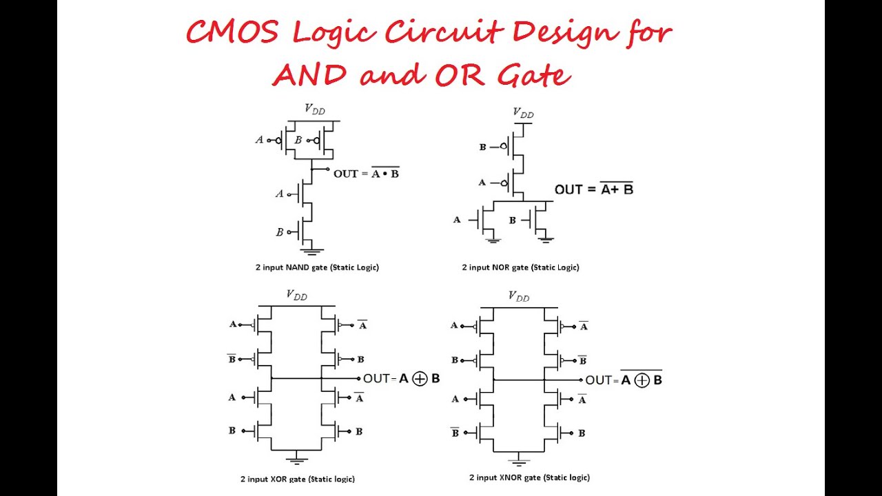
CMOS Logic Circuit Design for AND and OR Gate

CMOS NAND Gate Explained: Circuit, Working, Implementation, and Truth Table

SE1x_2022_Week_2_7_Semiconductor_Junction_The_Solar_Cell-video

Fixed-Bias Configuration of JFET (Graphical Approach)

Manufacturing Metrics | Performance and Cost

Manufacturing Systems | Industrial Automation
5.0 / 5 (0 votes)
