Persambungan Semikonduktor PN pada Dioda | Kuliah Fisika Semikonduktor
Summary
TLDRThis video explains the basic principles of a PN junction diode, focusing on the interaction between P-type and N-type semiconductors. It covers key concepts such as depletion layers, diffusion of electrons and holes, and the effects of applying forward or reverse bias. The video describes how the depletion layer expands in reverse bias, preventing current flow, and narrows in forward bias, allowing current to pass through. Additionally, it touches on the energy band diagrams associated with these processes and the threshold voltage required for current to flow in a forward-biased diode.
Takeaways
- 💡 The lesson is about the P-N junction in diodes, focusing on the interaction between P-type and N-type semiconductors.
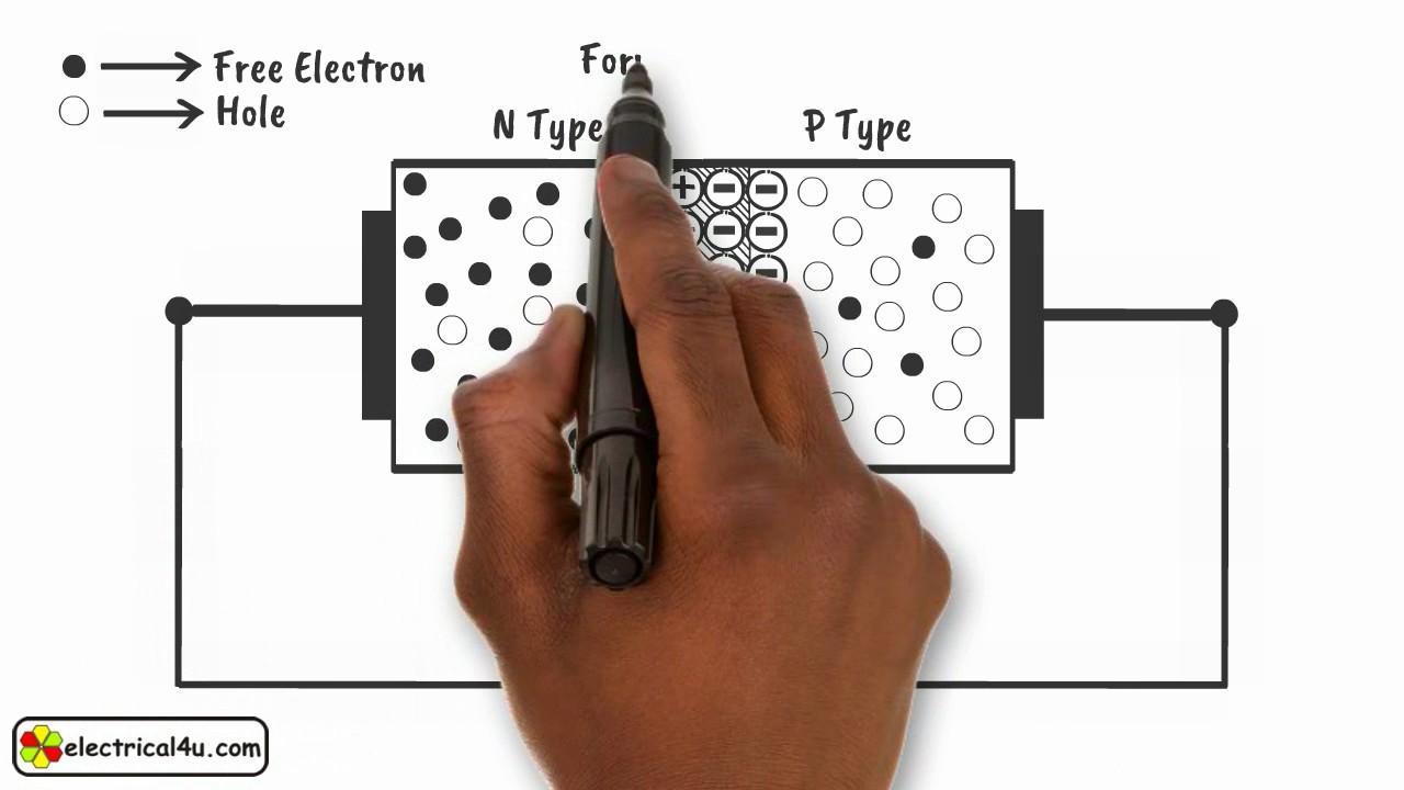
- 🔋 When no voltage is applied (Zero Bias), a depletion layer forms due to diffusion of majority carriers.
- 🌐 Electrons from the N-type semiconductor diffuse to the P-type, leaving behind positive ions.
- ➖ Holes from the P-type semiconductor diffuse to the N-type, leaving behind negative ions, forming the depletion layer.
- ⚡ The electric field created by the depletion layer opposes further diffusion of electrons and holes.
- 🔄 In Reverse Bias, when the P-side is connected to a negative voltage and the N-side to positive, the depletion layer widens, preventing current flow.
- 💻 The energy band diagram shows an increasing barrier for electron flow in reverse bias due to the widening depletion layer.
- 🔋 In Forward Bias, when the P-side is connected to positive voltage and N-side to negative, the depletion layer becomes thinner, allowing current to flow.
- ⚙️ The forward voltage must be greater than a certain threshold (typically 0.7V for silicon) to allow current to flow in a diode.
- 📈 The diode conducts current in one direction under forward bias, and no current flows under reverse bias, which is a key characteristic of diodes.
Q & A
What is a PN junction in a semiconductor?
-A PN junction is the boundary created when a p-type semiconductor is joined with an n-type semiconductor. This junction allows for controlled current flow depending on the voltage applied across the junction.
What is the depletion layer in a PN junction?
-The depletion layer forms at the PN junction due to the diffusion of electrons from the n-type region to the p-type region and holes from the p-type region to the n-type region. This results in a region with no free charge carriers, acting as a barrier to further diffusion.
How does an electric field form in the depletion layer?
-An electric field forms in the depletion layer due to the separation of charges. The diffusion of electrons and holes leaves behind positively charged ions in the n-type region and negatively charged ions in the p-type region, creating an electric field that opposes further diffusion.
What happens to the depletion layer under zero bias (no applied voltage)?
-Under zero bias, the depletion layer remains stable, and no current flows through the PN junction because the electric field prevents the movement of electrons and holes across the junction.
What occurs when a reverse bias is applied to a PN junction?
-In reverse bias, the p-type semiconductor is connected to the negative terminal and the n-type to the positive terminal. This widens the depletion layer, increasing the energy barrier and preventing current flow through the junction.
Why does the depletion layer widen under reverse bias?
-The depletion layer widens under reverse bias because the applied voltage increases the separation between the positive and negative charges, making it harder for electrons and holes to recombine, thereby increasing the energy barrier for current flow.
What happens to the current flow in reverse bias?
-In reverse bias, no significant current flows through the PN junction. Only a very small leakage current might flow due to minority carriers, but overall, the current is negligible.
What occurs when forward bias is applied to a PN junction?
-In forward bias, the p-type semiconductor is connected to the positive terminal and the n-type to the negative terminal. This reduces the width of the depletion layer, allowing current to flow through the junction.
Why is there a minimum voltage required for current flow in forward bias?
-A minimum voltage, known as the threshold or cut-in voltage (around 0.7V for silicon diodes), is required in forward bias to overcome the potential barrier created by the depletion layer and allow electrons and holes to move across the junction.
What is the behavior of a diode in forward and reverse bias?
-In forward bias, a diode allows current to flow easily once the threshold voltage is reached. In reverse bias, it prevents current from flowing, except for a tiny leakage current. This makes diodes useful for allowing current to flow in only one direction.
Outlines

Dieser Bereich ist nur für Premium-Benutzer verfügbar. Bitte führen Sie ein Upgrade durch, um auf diesen Abschnitt zuzugreifen.
Upgrade durchführenMindmap

Dieser Bereich ist nur für Premium-Benutzer verfügbar. Bitte führen Sie ein Upgrade durch, um auf diesen Abschnitt zuzugreifen.
Upgrade durchführenKeywords

Dieser Bereich ist nur für Premium-Benutzer verfügbar. Bitte führen Sie ein Upgrade durch, um auf diesen Abschnitt zuzugreifen.
Upgrade durchführenHighlights

Dieser Bereich ist nur für Premium-Benutzer verfügbar. Bitte führen Sie ein Upgrade durch, um auf diesen Abschnitt zuzugreifen.
Upgrade durchführenTranscripts

Dieser Bereich ist nur für Premium-Benutzer verfügbar. Bitte führen Sie ein Upgrade durch, um auf diesen Abschnitt zuzugreifen.
Upgrade durchführenWeitere ähnliche Videos ansehen

How a DIODE Works?

Basic Electronics: PN Junction Working Principle and V-I Characteristics of PN Junction Diode
How does a Diode Work? A Simple Explanation | How Diodes Work | Electrical4U

How does a P-N Junction Diode works? Explained through Animation

VI Characteristics of PN Junction Diode | PN Junction Forward Bias | PN Junction Reverse Bias
U1_L2_P-N Junction Diode | Electronics Engineering (BEC101/201)| Hindi
5.0 / 5 (0 votes)
