Microfabrication with Glass-Like Carbon
Summary
TLDRThis script delves into microfabrication using glass-like carbon, emphasizing the benefits of smaller structures for quality and thermal management. It discusses challenges like trapped bubbles and impurities in larger structures, advocating for microscale fabrication for better carbon quality and efficient defect annealing. The speaker explores various microfabrication techniques, including traditional methods like drilling and EDM, and advanced lithographic processes. The goal is to create microscale devices with high surface area for enhanced functionality in sensors and batteries, while also touching on the distinction between microscale structures and devices.
Takeaways
- 🔬 Micro scale structures are those in the micrometer size range, and their quality can be optimized by reducing their size to allow for better annealing of defects and trapped bubbles.
- 🌡️ Heat treatment temperatures can be lowered for smaller structures due to increased surface area, which facilitates the annealing process and reduces impurities.
- 💧 Defects in carbon structures, such as non-six-membered rings, are higher energy structures that can anneal out to form more energetically favorable six-membered rings, leading to a more graphitic order.
- 🧊 The transition from large to smaller structures (from centimeter to millimeter, and micro to nano) is beneficial for material quality and allows for batch fabrication, reducing material use and increasing efficiency.
- 🔋 Smaller structures have a higher surface area to volume ratio, which is advantageous for applications like biosensors and batteries where interaction with the environment is crucial.
- 🏭 Industrial glassy carbon devices or large scale structures should ideally be smaller than 5 millimeters to maintain optimal properties.
- 🔩 Microfabrication techniques are specialized and differ from traditional manufacturing methods, often involving photolithography and other non-traditional methods to create microscale structures.
- 📡 MEMS (Micro Electro Mechanical Systems) are a class of microscale devices that utilize mechanical properties to obtain electrical signals or vice versa, but not all microscale devices are MEMS.
- ⚙️ Traditional manufacturing techniques like drilling, EDM, and ECM can also be adapted for microfabrication, showing the versatility in approach to creating microscale structures.
- 🔬 Lithographic techniques such as photolithography, electron beam lithography, and nano imprint lithography are crucial for patterning polymers in microfabrication processes.
Q & A
What are microscale structures in the context of manufacturing with glass-like carbon?
-Microscale structures refer to structures that are in the micrometer size range, which can be created using glass-like carbon through various microfabrication techniques.
Why might large structures made of polymers have bubbles when converted into carbon?
-Large structures made of polymers may have bubbles trapped inside due to byproducts like tar-like materials and synthetic gases released during pyrolysis. The large size of these structures can prevent efficient annealing of these bubbles.
How does the thermal conductivity of a carbonizing matrix affect the quality of glassy carbon structures?
-The thermal conductivity of a carbonizing matrix can vary, with higher carbon fractions leading to increased conductivity. However, impurities and trapped bubbles in the core can lower thermal conductivity, affecting the overall quality of the glassy carbon structure.
What is the optimum size for industrial glassy carbon devices to avoid issues related to trapped bubbles and impurities?
-The optimum size for industrial glassy carbon devices or large scale structures is smaller than 5 millimeters to minimize issues related to trapped bubbles and impurities.
Why is it beneficial to reduce the size of structures from centimeter to millimeter, and further to micrometer or nanometer?
-Reducing the size of structures allows for better quality carbon due to lower heat treatment temperatures required for annealing out byproducts and defects, and it also increases the surface area to volume ratio, which is beneficial for various applications.
What is the significance of a higher surface area in microscale structures for sensor applications?
-A higher surface area in microscale structures is significant for sensor applications as it allows for better capture of target molecules, even at low concentrations, due to increased contact with the surrounding liquid.
How does the size reduction of devices impact their functionality and sensitivity in applications like batteries?
-Reducing the size of devices can lead to a higher surface area, which is beneficial for applications like lithium-ion batteries. This allows for more efficient charging and discharging as ions can move in and out of the structure more effectively.
What are the requirements for a polymer to be used in microfabrication for creating glass-like carbon structures?
-A polymer used in microfabrication for creating glass-like carbon structures should undergo coking without becoming too soft to lose shape, have a high carbon content, and be compatible with both the fabrication techniques and the carbonization process.
Why is batch fabrication preferred in microfabrication processes?
-Batch fabrication is preferred in microfabrication because it allows for the creation of multiple structures or devices at once, which is more efficient and cost-effective compared to individual, serial manufacturing techniques.
What is the difference between microscale structures and microscale devices?
-Microscale structures are physical forms at the micrometer scale, while microscale devices are systems that perform a specific function or operation at the microscale, with their functional elements being smaller than 100 micrometers.
How do top-down and bottom-up approaches differ in microfabrication?
-Top-down approaches in microfabrication involve starting with a larger piece of material and removing unnecessary parts, while bottom-up approaches build structures by adding layers or components, starting from smaller molecules or cells.
Outlines

Dieser Bereich ist nur für Premium-Benutzer verfügbar. Bitte führen Sie ein Upgrade durch, um auf diesen Abschnitt zuzugreifen.
Upgrade durchführenMindmap

Dieser Bereich ist nur für Premium-Benutzer verfügbar. Bitte führen Sie ein Upgrade durch, um auf diesen Abschnitt zuzugreifen.
Upgrade durchführenKeywords

Dieser Bereich ist nur für Premium-Benutzer verfügbar. Bitte führen Sie ein Upgrade durch, um auf diesen Abschnitt zuzugreifen.
Upgrade durchführenHighlights

Dieser Bereich ist nur für Premium-Benutzer verfügbar. Bitte führen Sie ein Upgrade durch, um auf diesen Abschnitt zuzugreifen.
Upgrade durchführenTranscripts

Dieser Bereich ist nur für Premium-Benutzer verfügbar. Bitte führen Sie ein Upgrade durch, um auf diesen Abschnitt zuzugreifen.
Upgrade durchführenWeitere ähnliche Videos ansehen

Glasherstellung - Das Floatverfahren (Saint-Gobain)
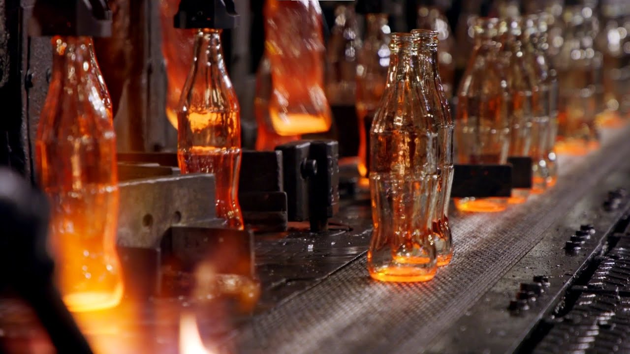
How It's Made Glass
Chapter 1 Part B: Structure and Bonding, acids and bases
Introduction to Modern Broiler Production (all subjects combined)

水草水槽の疑問にお答えします!AQUASHOP wasabi Q&Aシリーズ ① 「流木のアク抜きって必要?エビが動かないんだけど?ガラス蓋ってしてもいい?」アクアリウム・熱帯魚・水草のノウハウ
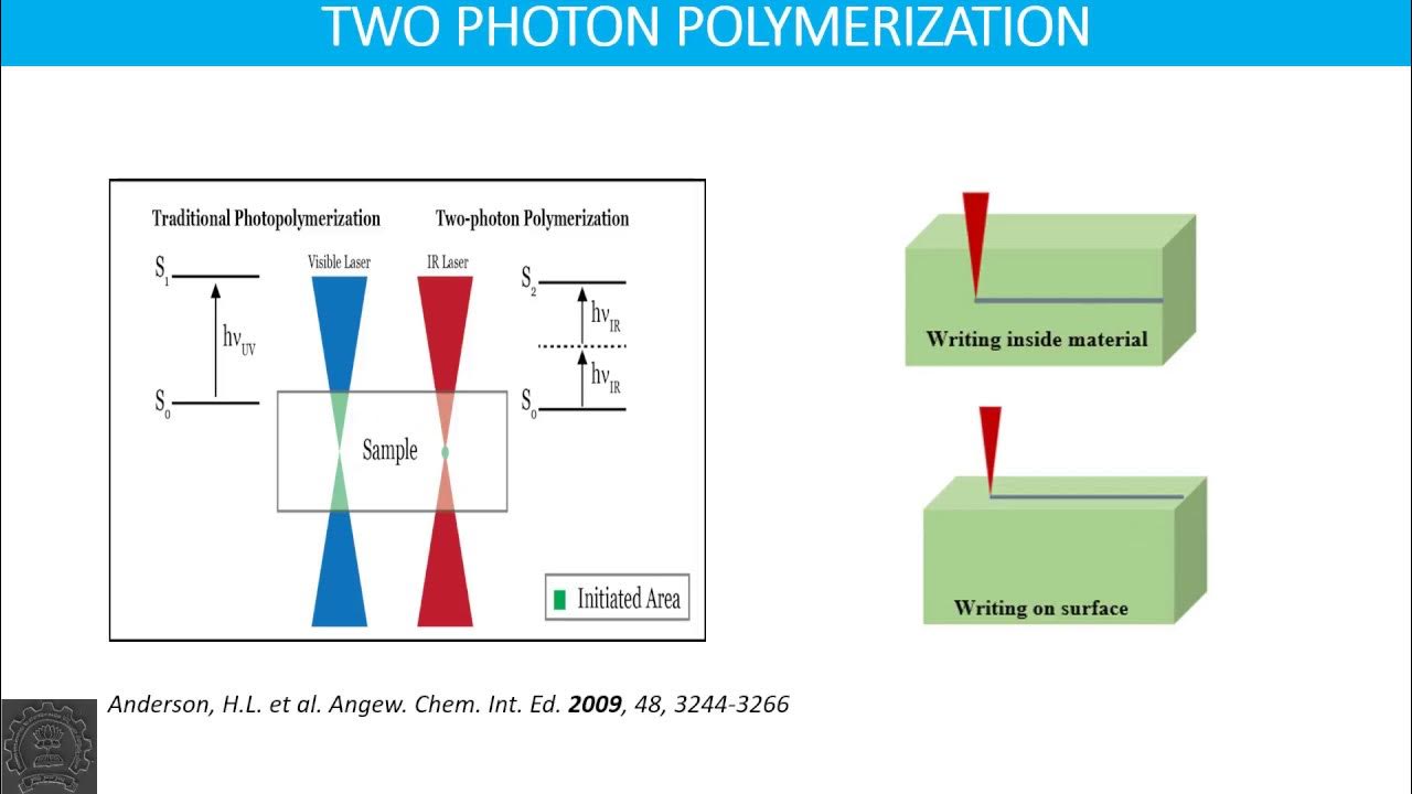
3D patterning using Two Photon Lithography
5.0 / 5 (0 votes)
