The Class A amplifier - build and test (2/2)
Summary
TLDRIn this educational video, the creator discusses designing, simulating, and building a single-transistor wideband common emitter amplifier. The goal is to deliver half a watt into a 50-ohm load using a BD135 NPN transistor. The video covers the calculation of components, biasing, and efficiency, followed by real-life testing to verify performance. The creator also uses a circuit simulator to ensure accuracy and discusses the amplifier's wide bandwidth and modulation capabilities. The video concludes with a thermal performance test and insights on improving efficiency.
Takeaways
- 🔬 The video focuses on designing, simulating, and building a Class A single-transistor wideband common emitter amplifier.
- 🎯 The design goal is to deliver half a watt into a 50-ohm load, using a BD135 medium power NPN transistor for amplification.
- 🔧 The amplifier configuration includes a resistor network for bias point setting, an emitter resistor for stability and negative feedback, and an inductor in the collector for efficiency.
- 🔌 The supply voltage is calculated to be 10 volts, considering the load, collector-emitter voltage drop, and emitter resistor voltage drop.
- 🔢 The static operating current is determined to be 141.5 milliamps, which is half of the peak current.
- ⚙️ The emitter resistor is calculated to be 3.3 ohms, and the biasing resistors are calculated to be 620 ohms and 91 ohms.
- 🌡️ The amplifier is expected to have a power dissipation of almost 1.5 watts, necessitating a heatsink for the transistor.
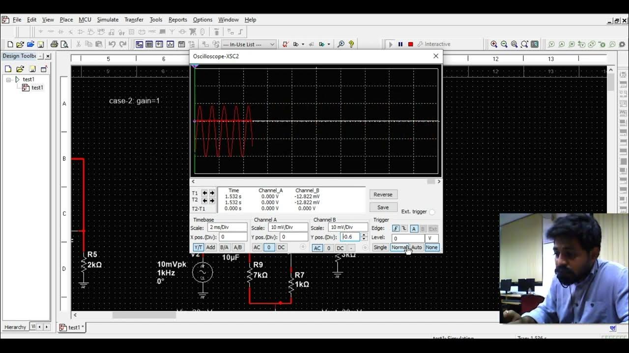
- 📊 Simulations show a voltage gain of about 13, an efficiency of 28.6%, and a bandwidth from 10 kHz to 10 MHz.
- 🔍 Real-life testing confirms the amplifier's performance, with a wide bandwidth and good modulation following for various types of signals.
- 🌡️ Thermal performance testing indicates the importance of considering heat dissipation not only for the transistor but also for other components.
Q & A
What is the main goal of designing the class A amplifier discussed in the script?
-The main goal is to design a single transistor wideband common emitter amplifier that can deliver half a watt into a 50-ohm load.
Why is a BD135 transistor chosen as the main amplifying element?
-The BD135 is chosen because it is a medium power NPN transistor with a high enough transition frequency to allow the amplifier to work up to a few megahertz.
What is the expected theoretical maximum efficiency of the amplifier design?
-The expected theoretical maximum efficiency of the amplifier design is 50%.
How is the output voltage calculated for the amplifier?
-The output voltage is calculated based on the output load value and the output power, requiring a 5-volt RMS voltage, which translates to a 14.14-volt peak-to-peak voltage.
What is the purpose of the emitter resistor in the amplifier circuit?
-The emitter resistor serves two purposes: it helps set the voltage gain of the circuit and provides a voltage drop that contributes to heat dissipation and circuit stability.
Why is an inductor placed in the collector of the amplifier?
-An inductor is placed in the collector to maximize efficiency by minimizing the voltage drop across the collector and emitter.
How is the static operating current determined for the amplifier?
-The static operating current is determined based on the peak-to-peak load voltage and the load value, which gives a peak current of 283 milliamps, and the static current is half of this value.
What is the significance of the biasing resistors in the circuit?
-The biasing resistors are used to set the operating point of the transistor and ensure stability by providing the right amount of base current.
How is the power dissipation calculated for the transistor?
-The power dissipation is calculated by considering the static power consumption of the amplifier, which is assumed to be mostly dissipated on the transistor, resulting in almost one and a half watts.
What is the expected efficiency of the amplifier based on simulations?
-The expected efficiency based on simulations is about 35%, which is derived from the output power and the input power calculations.
How is the bandwidth of the amplifier tested and what are the results?
-The bandwidth is tested using an AC simulation, and the results show a flat response from around 10 kHz up to around 10 MHz, indicating a wide bandwidth amplifier.
Outlines

هذا القسم متوفر فقط للمشتركين. يرجى الترقية للوصول إلى هذه الميزة.
قم بالترقية الآنMindmap

هذا القسم متوفر فقط للمشتركين. يرجى الترقية للوصول إلى هذه الميزة.
قم بالترقية الآنKeywords

هذا القسم متوفر فقط للمشتركين. يرجى الترقية للوصول إلى هذه الميزة.
قم بالترقية الآنHighlights

هذا القسم متوفر فقط للمشتركين. يرجى الترقية للوصول إلى هذه الميزة.
قم بالترقية الآنTranscripts

هذا القسم متوفر فقط للمشتركين. يرجى الترقية للوصول إلى هذه الميزة.
قم بالترقية الآنتصفح المزيد من مقاطع الفيديو ذات الصلة

Common-Emitter Configuration of a Transistor
Multisim Tutorials --2: CE amplifier simulation part 1
Transistor Biasing: What is Q-point? What is Load Line? Fixed Bias Configuration Explained
Darlington Pair Explained | The Darlington Pair as a Switch
Multistage Amplifier: Design Example
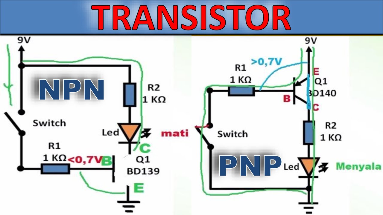
Penjelasan Transistor NPN dan PNP – Beserta contoh rangkaiannya
5.0 / 5 (0 votes)
