What is VLSI | Introduction & Design flow | VLSI | Lec-01
Summary
TLDRThis video introduces VLSI (Very Large Scale Integration), a key subject for BTech students, focusing on how integrated circuits (ICs) are fabricated to perform multiple operations using billions of transistors. The script explains the technology behind VLSI, particularly CMOS (Complementary Metal-Oxide-Semiconductor), known for its low power consumption and high packing density. The video also covers the VLSI design flow, which guides engineers through the process from design specification to fabrication, highlighting essential steps such as architecture design, gate-level design, and simulation. Overall, the video offers a comprehensive overview of the significance and process of VLSI design.
Takeaways
- 😀 VLSI stands for Very Large Scale Integration, which refers to the process of fabricating integrated circuits with millions of transistors.
- 😀 VLSI is studied by BTech students, typically in their third year or second semester, depending on the university.
- 😀 Integrated circuits (ICs) are used in various electronic devices like smartphones, smartwatches, LED/LCD TVs, and more.
- 😀 VLSI allows a single chip to perform multiple functions, thanks to the billions of transistors embedded within.
- 😀 The technology used to fabricate VLSI is CMOS (Complementary Metal-Oxide Semiconductor) technology, which is known for high packing density and low power consumption.
- 😀 CMOS technology is particularly advantageous for devices like smartwatches, which can last several days on a single charge, and energy-efficient TVs.
- 😀 VLSI design flow involves a step-by-step process starting from design specification to fabrication of the final product.
- 😀 The VLSI design flow includes stages like architecture design, gate-level design, circuit-level design, and hardware description language (HDL) coding.
- 😀 In the HDL coding stage, designers use languages like VHDL and Verilog to describe the behavior of the circuits.
- 😀 Simulation and verification are critical stages in the VLSI design flow to ensure the circuit meets the specified requirements before fabrication.
- 😀 If any issues arise during verification, designers revisit the HDL coding and make necessary adjustments to meet the required outputs.
Q & A
What does VLSI stand for?
-VLSI stands for Very Large Scale Integration. It refers to the process of creating integrated circuits by combining a large number of transistors into a single chip.
What is the importance of VLSI in modern electronics?
-VLSI is important because it enables the creation of highly compact and efficient integrated circuits that power many modern devices like smartphones, smartwatches, LED TVs, and other electronic gadgets.
What is the key feature of VLSI technology?
-The key feature of VLSI technology is its ability to integrate millions of transistors into a single chip, allowing it to perform multiple functions and operations, which is critical for modern electronics.
What are the different types of IC technologies mentioned?
-The different types of IC technologies mentioned are Small Scale Integration (SSI), Medium Scale Integration (MSI), Large Scale Integration (LSI), Very Large Scale Integration (VLSI), Ultra Large Scale Integration (ULSI), and Giant Scale Integration (GSI).
Which technology is best suited for the fabrication of VLSI circuits?
-CMOS (Complementary Metal-Oxide Semiconductor) technology is best suited for the fabrication of VLSI circuits due to its high packing density and low power consumption.
What are the advantages of CMOS technology in VLSI?
-The advantages of CMOS technology in VLSI include high packing density and very low power consumption, making it ideal for devices like smartphones and LED TVs that need to operate efficiently on low power.
What does the VLSI design flow describe?
-The VLSI design flow describes the step-by-step process of designing an integrated circuit, starting from market requirements and design specifications, moving through architecture design, gate-level design, HDL coding, simulation, verification, and finally, fabrication.
What is the role of simulation in the VLSI design process?
-Simulation in the VLSI design process is used to verify the behavior of the circuit by testing it with various input conditions to ensure the design functions as expected before moving to the fabrication stage.
What are the two main types of Hardware Description Languages (HDLs) used in VLSI design?
-The two main types of Hardware Description Languages (HDLs) used in VLSI design are VHDL (Very High-Speed Integrated Circuit Hardware Description Language) and Verilog HDL.
What happens if the design does not meet the expected requirements after verification?
-If the design does not meet the expected requirements after verification, it is sent back to the HDL coding stage where modifications are made. The process continues iteratively until the design satisfies the original specifications.
Outlines

此内容仅限付费用户访问。 请升级后访问。
立即升级Mindmap

此内容仅限付费用户访问。 请升级后访问。
立即升级Keywords

此内容仅限付费用户访问。 请升级后访问。
立即升级Highlights

此内容仅限付费用户访问。 请升级后访问。
立即升级Transcripts

此内容仅限付费用户访问。 请升级后访问。
立即升级浏览更多相关视频

L1 | Era of Integrated Circuits | VLSI Technology (KEC053) | Hindi

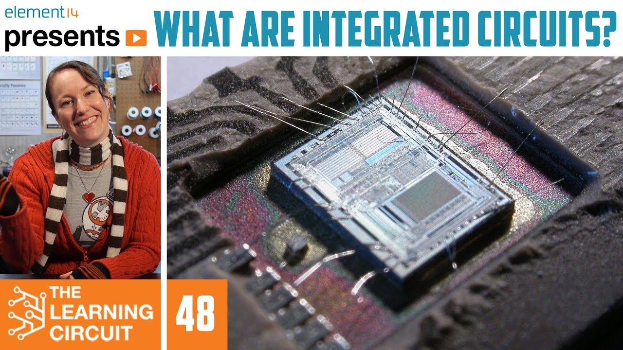
How Integrated Circuits Work - The Learning Circuit

The Basics of Electrical Components || Program Studi Teknik Elektro - MK : Bahasa Inggris

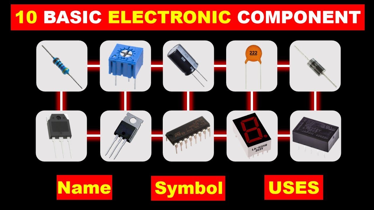
10 Basic Electronics Components and their functions @TheElectricalGuy

Silicon Run II

Difference between Embedded Systems vs VLSI Design in Telugu | Which is better for Career?
5.0 / 5 (0 votes)
