How are microchips made? - George Zaidan and Sajan Saini
Summary
TLDRThis script unveils the astonishing world inside computer chips, where billions of microscopic transistors form intricate, city-like structures that power modern technology. It explains how advanced techniques like photolithography use light to build these components with extreme precision, enabling the mass production of over a trillion chips each year. However, behind this technological marvel lies a resource-intensive process, consuming vast amounts of energy, water, and chemicals while generating significant waste and environmental risks. As demand for computing grows, the challenge becomes clear: future chip manufacturing must become more sustainable to balance innovation with environmental responsibility.
Takeaways
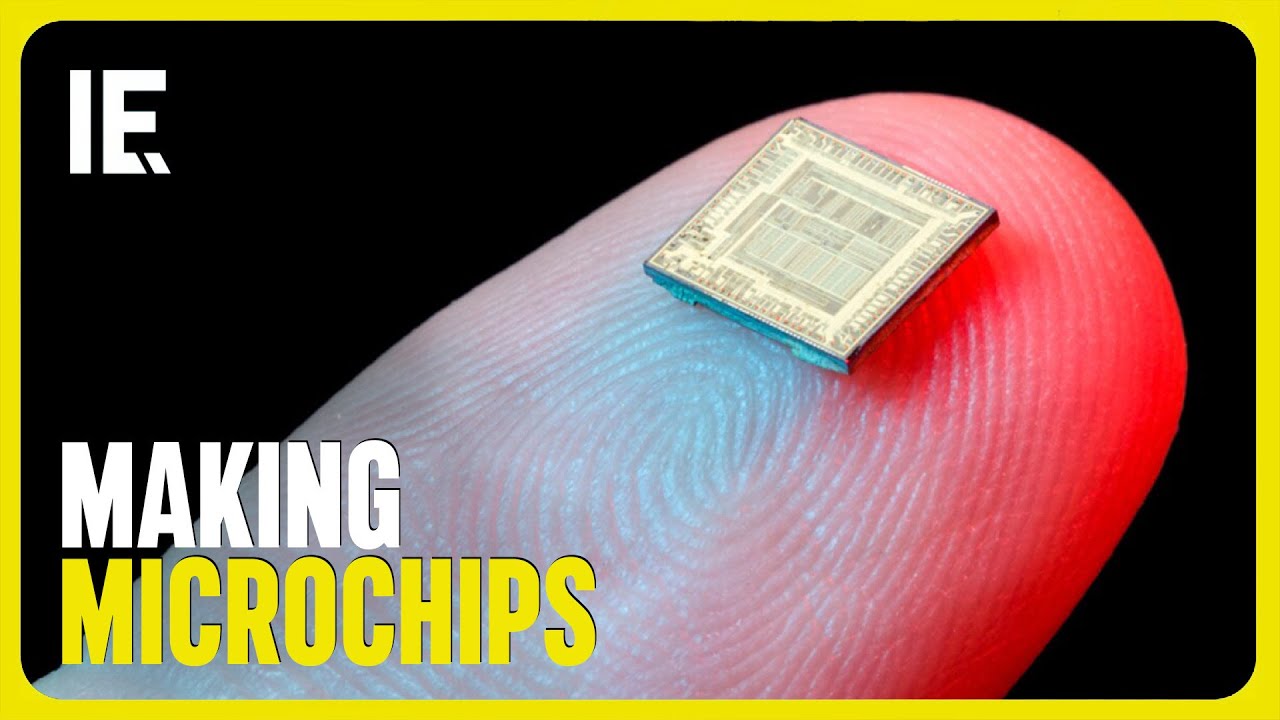
- 😀 A computer chip magnified 500 times reveals a complex 'city' of transistors linked by ultra-thin copper lines.
- 😀 Transistors, as small as 20 nanometers, act as switches that allow current to flow when they receive a voltage.
- 😀 More than 50 billion transistors can fit on a single chip, and globally, more than a trillion chips are produced each year.
- 😀 The process of building such tiny devices involves photolithography, a technique that uses light to construct all the devices at once.
- 😀 Silicon wafers are cleaned and then undergo a series of steps, including etching, photoresist coating, and ion implantation to form transistors.
- 😀 Chemical mechanical polishing (CMP) is used to smooth the wafer's surface with near-atomic precision, enabling further layers to be added.
- 😀 Fabs, or fabrication plants, operate 24/7 to transform raw silicon into chips in around three months, using vast amounts of electricity, water, and chemicals.
- 😀 The fabrication process generates significant waste, including chemical byproducts and water waste, which need extensive treatment.
- 😀 The use of PFAS-based photoresists is essential for creating smaller features on chips, but it poses environmental and health risks due to its persistence in the environment.
- 😀 As computing complexity increases, the demand for copper and precious metals also rises, leading to sustainability challenges in chip production.
- 😀 Future fabs will need to operate more sustainably, using smarter technologies to reduce their environmental impact and meet growing chip demand.
Q & A
What is the main purpose of a transistor in a computer chip?
-A transistor is a switch that controls the flow of electrical current. It allows current to flow when it receives a voltage, forming the fundamental building block of a chip's logic gates.
How small can transistors get on modern computer chips?
-Transistors can be as small as 20 nanometers, and over 50 billion of them can be packed onto a single chip.
What role does photolithography play in chip manufacturing?
-Photolithography is a crucial technology used to build all the tiny devices on a chip simultaneously. It uses light to measure and sculpt the features of the chip, creating patterns through selective illumination of a photoresist layer on a silicon wafer.
How does a silicon wafer get prepared before the chip pattern is imprinted?
-The silicon wafer is first cleaned with solvents and acids, then undergoes a heating process in a furnace to form a layer of silicon dioxide. Afterward, a photoresist is applied and hardened to prepare it for exposure to ultraviolet light.
What happens after the silicon wafer is exposed to ultraviolet light?
-The ultraviolet light weakens the chemical bonds in the photoresist layer in specific areas, allowing those parts to be washed away by a chemical solution. This reveals a pattern that is then etched onto the wafer surface.
What are the steps involved in etching the wafer surface?
-After the weakened photoresist is washed away, reactive gases in an etching machine remove the exposed silicon dioxide, creating windows that drill down into the wafer. This forms the underlying structure of the chip's components.
Why is chemical mechanical polishing (CMP) necessary in chip fabrication?
-CMP is used to smooth out the uneven surfaces created during the etching process. It flattens the 'hill-and-valley' features on the wafer to ensure that subsequent layers, such as copper lines, are laid down evenly.
How long does it take to transform a silicon wafer into chips?
-The process of transforming a single silicon wafer into hundreds of chips takes about three months, with continuous operation in fabrication plants.
What environmental impacts are associated with semiconductor fabrication?
-The fabrication of chips consumes vast amounts of electricity, water, solvents, acids, and precious metals. It also generates substantial liquid waste, such as wastewater from cleaning and CMP processes, and contributes to greenhouse gas emissions.
What are the sustainability challenges faced by semiconductor fabrication plants (fabs)?
-As demand for chips grows, fabs are pushing against sustainability limits. Issues like water scarcity, the use of harmful PFAS chemicals, and the consumption of vast resources for chip production are raising environmental concerns, requiring smarter and greener manufacturing practices.
Outlines

This section is available to paid users only. Please upgrade to access this part.
Upgrade NowMindmap

This section is available to paid users only. Please upgrade to access this part.
Upgrade NowKeywords

This section is available to paid users only. Please upgrade to access this part.
Upgrade NowHighlights

This section is available to paid users only. Please upgrade to access this part.
Upgrade NowTranscripts

This section is available to paid users only. Please upgrade to access this part.
Upgrade NowBrowse More Related Video

Transistors - The Invention That Changed The World

Bagaimana Cara Kerja Komponen Pada Komputer? 🖥 Menelusuri Cara Kerja Hardware pada PC

Bagaimana Komponen pada Komputer Bekerja? 🖥 Mari Bongkar Semua Hardware pada PC

How Computers Work: Circuits & Logic

INTRODUCTION AU LANGAGE BINAIRE
💻 How Are Microchips Made?
5.0 / 5 (0 votes)