Hoạt động của tiếp xúc P-N | Chất bán dẫn là gì?
Summary
TLDRThis video explains the structure and working principles of PN junctions, which are crucial components in semiconductors. It describes how P-type and N-type materials are formed by doping silicon with elements like Boron and Phosphorus, respectively. The video also explores how these materials conduct electricity via electrons and 'holes,' detailing the behavior of PN junctions in different conditions, including forward and reverse bias. It covers concepts such as depletion zones, electron movement, and how these mechanisms allow semiconductors to regulate electrical flow.
Takeaways
- 🟢 PN junctions (semiconductor junctions) are formed from two semiconductor layers of different types (P-type and N-type) to create an active electronic device.
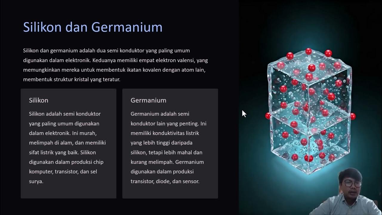
- 🟡 Semiconductor materials, such as silicon, are doped with impurities like Boron (for P-type) and Phosphorus (for N-type) to alter their electrical conductivity.
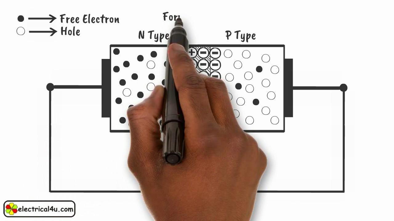
- 🔵 P-type semiconductors conduct electricity using 'holes' (absence of electrons), while N-type semiconductors conduct through electrons.
- ⚪ The interaction at the PN junction forms a depletion region, where positive and negative charges neutralize, leaving a zone with no free charge carriers.
- ⚫ The depletion region creates a barrier potential, typically around 0.7 volts for silicon, which affects the junction's behavior under different biases.
- 🟠 When forward-biased (positive voltage on the P-side), the depletion region shrinks, allowing current to flow through the junction.
- 🔴 When reverse-biased (positive voltage on the N-side), the depletion region widens, preventing current from flowing and blocking the junction.
- 🟣 Electrons and holes recombine in the depletion region, and this process governs the behavior of PN junctions in devices like diodes and transistors.
- 🟡 In a forward-biased junction, electrons flow from the N-type side, while holes flow from the P-type side, creating a current.
- 🔷 In reverse bias, no significant current flows due to the widening depletion region, making it useful for rectification and voltage control.
Q & A
What is a PN junction, and why is it important in semiconductor devices?
-A PN junction is the boundary between P-type and N-type semiconductors. It is critical in semiconductor devices because it allows the control of electrical current, forming the basis for components like diodes and transistors.
What materials are typically used to create P-type and N-type semiconductors?
-P-type semiconductors are created by doping silicon with Boron, while N-type semiconductors are made by doping silicon with Phosphorus. These materials adjust the electrical properties of silicon to allow it to conduct electricity.
How does a PN junction diode work in forward bias?
-In forward bias, the P-type side is connected to a positive voltage and the N-type side to a negative voltage. This reduces the potential barrier, allowing charge carriers (electrons and holes) to move across the junction, thus allowing current to flow.
What happens when a PN junction is reverse biased?
-When reverse biased, the P-type side is connected to a negative voltage and the N-type side to a positive voltage, increasing the potential barrier. This widens the depletion region, preventing current flow except for a small leakage current.
What is the depletion region in a PN junction?
-The depletion region is the area around the PN junction where mobile charge carriers (electrons and holes) have diffused and neutralized each other, leaving behind immobile ions. This region acts as an insulator, preventing current flow under normal conditions.
Why does the depletion region form at the PN junction?
-The depletion region forms because when P-type and N-type materials are brought together, electrons from the N-side combine with holes from the P-side near the junction. This results in a region depleted of charge carriers, creating an electric field that opposes further charge movement.
What role do Boron and Phosphorus play in semiconductor doping?
-Boron, when added to silicon, creates a P-type semiconductor by introducing 'holes' (positive charge carriers). Phosphorus introduces extra electrons, creating an N-type semiconductor. These materials control the type and number of charge carriers available.
What is the significance of the 0.7V threshold in a silicon PN junction diode?
-The 0.7V threshold is the minimum voltage required to overcome the built-in potential of a silicon PN junction diode in forward bias, allowing current to flow. Below this voltage, the diode remains non-conductive.
What is the difference between electron and hole conduction in semiconductors?
-Electron conduction occurs when negatively charged electrons move through the material, common in N-type semiconductors. Hole conduction occurs when positively charged 'holes' (absence of electrons) move, which is typical in P-type semiconductors.
How does doping affect the electrical conductivity of silicon?
-Doping silicon with impurities like Boron (for P-type) or Phosphorus (for N-type) alters its electrical conductivity. Doping increases the number of charge carriers (electrons or holes), allowing silicon to conduct electricity more effectively.
What is the role of the depletion layer in preventing current flow in reverse bias?
-In reverse bias, the depletion layer becomes wider, which increases resistance and prevents current flow. The widened depletion region acts as an insulator, blocking the flow of electrons and holes across the junction.
Outlines

Этот раздел доступен только подписчикам платных тарифов. Пожалуйста, перейдите на платный тариф для доступа.
Перейти на платный тарифMindmap

Этот раздел доступен только подписчикам платных тарифов. Пожалуйста, перейдите на платный тариф для доступа.
Перейти на платный тарифKeywords

Этот раздел доступен только подписчикам платных тарифов. Пожалуйста, перейдите на платный тариф для доступа.
Перейти на платный тарифHighlights

Этот раздел доступен только подписчикам платных тарифов. Пожалуйста, перейдите на платный тариф для доступа.
Перейти на платный тарифTranscripts

Этот раздел доступен только подписчикам платных тарифов. Пожалуйста, перейдите на платный тариф для доступа.
Перейти на платный тарифПосмотреть больше похожих видео

SEMICONDUCTOR | what is SEMICONDUCTOR | css general science and ability | by ibrar ahmad

Lab 4 and 5: PN junctions and Solar Cells

003 INFORMASI: Pengetahuan Dasar Semikonduktor?
Pengantar Semi Konduktor

How LED Works - Unravel the Mysteries of How LEDs Work!
How does a Diode Work? A Simple Explanation | How Diodes Work | Electrical4U
5.0 / 5 (0 votes)
