PIC16 Microcontrollers, Unit 3, Ch 2.1-2.2; Block Diagram & Status Register
Summary
TLDRClint Halstead's lecture introduces the PIC mid-range family of microprocessors, focusing on the PIC16F877A. The lecture covers the architecture, memory types including SRAM, EEPROM, and program memory, as well as special function registers. It highlights the simplicity of the 16F84A as a learning platform due to its direct applicability to larger microprocessors. The differences between various models, including the 16F84A, 16LF80A, and 16F87, are discussed, emphasizing the increased capabilities of the latter. The lecture also touches on the importance of the status register in indicating the result of ALU operations.
Takeaways
- 😀 The lecture is an introduction to microprocessors, focusing on the PIC mid-range family and specifically the 16F84A model.
- 📚 The reference material for the lecture is 'Microprocessors and Microcontrollers: Applications and Programming' by Tim Worrell, specifically the second edition.
- 💡 The 16F84A is chosen for its simplicity, making it easier for students to learn the fundamentals applicable to more complex microprocessors.
- 🔢 The 16F84A has 18 pins, operates at up to 20 megahertz, and includes 1k of program memory, 68 bytes of RAM, and 64 bytes of EEPROM.
- 🔌 The microprocessor features include an 8-bit timer, a 5-bit parallel port, and in-circuit serial programming (ISP).
- 🚀 Learning starts with the 16F84A and progresses to more advanced models like the 16F87 and 88, which add more peripherals.
- 🔋 The 16F87 model increases program memory to 4k, RAM to 368 bytes, and EEPROM to 256 bytes, and adds additional features like two parallel ports and more peripherals.
- 🔧 The 16F84A-4 variant has a different clock range, only going up to 4 megahertz, and an extended supply voltage range.
- 🔄 The 16F84 has a 10-bit ADC with multiplex capabilities, allowing one ADC to switch between different channels.
- 🔗 The block diagram of the 16F84A shows enhancements over previous models, including a 13-bit address bus and an increased stack level.
- 🛠 The status register is crucial for indicating the result of ALU operations, with specific bits for zero, digital carry, and carry out.
Q & A
What is the main topic of Clint Halstead's lecture?
-The main topic of Clint Halstead's lecture is an introduction to microprocessors, specifically focusing on the PIC mid-range family and the 16F877A microcontroller from the book 'Microprocessors and Microcontrollers: Applications and Programming' by Tim Worrell.
Why is the 16F84A microcontroller chosen for the class?
-The 16F84A microcontroller is chosen for the class because it is one of the simplest chips, making it easier for students to learn the fundamentals of microprocessors. The knowledge gained from studying this microcontroller is directly applicable to larger microprocessors as it forms part of their core.
What are the three different memory areas mentioned in the lecture?
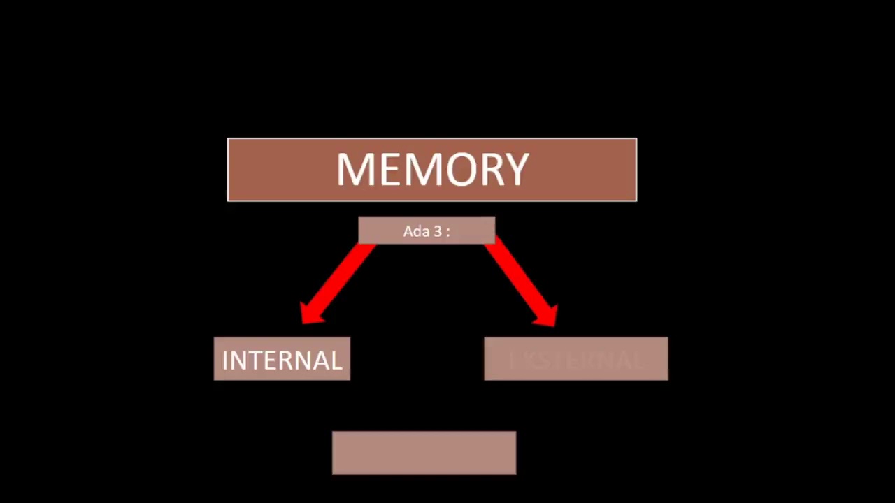
-The three different memory areas mentioned in the lecture are SRAM (Static Random Access Memory), EEPROM (Electrically Erasable Programmable Read-Only Memory), and Program Memory (flash memory).
What does ISP stand for in the context of the 16F84A microcontroller?
-ISP stands for In-Circuit Serial Programming, which is a feature of the 16F84A microcontroller that allows for programming the device through two pins using a USB module connected to a computer.
What are the differences between the 16F84A and the 16LF80A?
-The main difference between the 16F84A and the 16LF80A is the extended supply voltage range in the 16LF80A. Everything else, such as the number of pins, program memory, and features, remains the same.
How does the 16F877A differ from the 16F84A in terms of program memory and peripherals?
-The 16F877A has quadruple the program memory compared to the 16F84A, allowing for larger code. It also has significantly more RAM, increased EEPROM size, and additional peripherals such as two parallel ports, three counter timers, a capture compare PWM module, two serial communication modules, and two download comparators.
What is the purpose of the status register in a microcontroller?
-The status register in a microcontroller is used to indicate the results of arithmetic or logic operations, such as whether there was an overflow (carry), whether the result is zero, and other condition code flags that help in understanding the outcome of operations performed by the ALU (Arithmetic Logic Unit).
What is the significance of the 'C' bit in the status register?
-The 'C' bit in the status register signifies a carry out from the most significant bit of the result. It is set to 1 if an overflow occurs during an arithmetic operation, indicating that the result is too large for the W register to hold accurately.
What is the role of the W register in the microcontroller?
-The W register, also known as the working register, serves as a scratchpad register where the results of ALU operations, such as addition, subtraction, and logical operations, are stored temporarily.
How does the block diagram of the 16F84A differ from the 12F508 part discussed in chapter 1?
-The block diagram of the 16F84A has a 13-bit address bus compared to the 12-bit address bus of the 12F508. It also has an increased program memory of 1K, an additional level in the stack, and an EEPROM section for non-volatile data storage.
What is the difference between RAM and EEPROM in terms of data retention?
-RAM is volatile memory, meaning data stored in it will be lost when power is disconnected. In contrast, EEPROM is non-volatile memory, retaining data even when the power is turned off.
Outlines
📘 Introduction to Microprocessors and PIC Mid-Range Family
Clint Halstead introduces the lecture on microprocessors, focusing on the PIC mid-range family, specifically the 16F877A. The lecture is based on Tim Worrell's book, 'Microprocessors and Microcontrollers: Applications and Programming', and covers chapters on the PIC mid-range family and the 16F84A. The 16F84A is chosen for its simplicity, making it an ideal starting point for learning, with its features applicable to more complex microprocessors. The chip has 18 pins, operates up to 20 MHz, and includes 1k of program memory, 68 bytes of RAM, and 64 bytes of EEPROM. The lecture will delve into the technical architecture, memory, status registers, and various other aspects of the microprocessor, but will only cover the first two sections of the book.
🔌 Enhanced Features of the PIC 16F Microprocessors
The second paragraph delves into the enhanced features of the PIC 16F microprocessors, including the 16F84A and its variants. The 16F84A has been expanded to include more peripherals and advanced technology, such as two parallel ports, three counter timers, capture compare PWM modules, two serial communication modules, and nano watt technology. It also includes a software-selectable oscillator block and in-circuit serial programming. The 16F84A-4 variant has a different clock range, while the 16F87 increases program memory and RAM, and adds more peripherals. The paragraph also discusses the pin connections and features of the 16F microprocessors, such as dedicated master clear and oscillator pins, and the addition of an interrupt pin.
💾 Memory and I/O Features of the PIC 16F Microprocessors
This paragraph discusses the memory and I/O features of the PIC 16F microprocessors, highlighting the distinction between program code stored in flash memory and data stored in RAM, which is volatile and lost when power is disconnected. The EEPROM is introduced as a non-volatile memory that retains data even when power is off. The paragraph also explains the 13-bit address bus and the increase in memory from 52K to 1K, as well as the addition of an eighth level stack. The I/O ports are described, with the LSB of port B shared with the interrupt feature, and the status register is introduced, which includes condition code flags to indicate overflow and other arithmetic results.
🛠 Status Register and Microprocessor Block Diagram
The final paragraph focuses on the status register and the block diagram of the microprocessor. The status register's role in indicating the result of arithmetic or logic operations is explained, with emphasis on the zero, carry, and other condition code flags. The block diagram is used to illustrate the flow of data and instructions within the microprocessor, including the instruction register, RAM registers, and decode register. The lecture concludes with a mention of continuing the discussion in the next video series, highlighting the importance of understanding the microprocessor's architecture for effective programming and application.
Mindmap
Keywords
💡Microprocessors
💡PIC16F877A
💡Memory
💡Status Register
💡SRAM
💡EEPROM
💡Program Memory
💡Special Function Registers
💡Oscillator
💡Power-On Reset
💡Interrupt
Highlights
Introduction to microprocessors with a focus on the PIC mid-range family.
Discussion of the PIC16F877A microcontroller and its application in learning due to its simplicity and foundational role in understanding more complex microprocessors.
Explanation of the 16F84A microcontroller's features, including its 18 pins, 20 MHz operation, and memory configurations.
The direct applicability of knowledge gained from studying the 16F84A to more advanced microprocessors with additional peripherals.
Introduction to the different memory areas of the 16F84A: program memory, SRAM, EEPROM, and their respective sizes.
Description of the 16F84A's peripherals, such as an 8-bit timer, parallel ports, and in-circuit serial programming (ICSP).
Comparison between the 16F84A and its variants, such as the LF and A-4 versions, highlighting differences in voltage range and clock speed.
Detailed comparison of the 16F87 with the 16F84A, emphasizing the increased program memory, RAM, EEPROM, and additional peripherals.
Introduction of advanced features in the 16F87, such as counter timers, capture compare PWM module, and serial communication modules.
Explanation of the nano watt technology and software selectable oscillator block in the 16F87 for improved power efficiency and flexibility.
Overview of the 16F848's additional features, including 10-bit ADC channels and their multiplexing capabilities.
Discussion on the importance of the master clear and dedicated oscillator pins for improved functionality and ease of use.
Introduction to the block diagram of the 16F84A, outlining its core components and their interconnections.
Explanation of the 13-bit address bus and its enhancement over previous models with a 12-bit address bus.
Description of the EEPROM section, its purpose, and how it differs from volatile RAM in terms of data retention.
Importance of the status register in indicating the result of ALU operations and its role in managing condition code flags.
Overview of the lecture's continuation in a subsequent video series, indicating ongoing education on the topic.
Transcripts
hello this is Clint Halstead and I am
giving a lecture on introduction to
micro processors and I will be using
will be discussing pic16f877a plication
second edition by Tim Worrell sureste
this chapter is chapter two introducing
the pic mid-range family and the sixteen
f-84 a this chapter aims to introduce
the pig mid-range family to talk about
the overall tech architecture of the 16
f-84 a the memory things like status
register SRAM
EEPROM doli prom program memory stacked
special function registers addressing
configuration word oscillator pipelining
power on reset reset master clear
powerup timing
this lecture will only cover the first
two sections of the book so let's let's
get started ok so it's after 29 in the
book it shows a table of several
different parts this list shown here is
not exhaustive is not the exact one of
the book it only shows the first few but
the first part we'll talk about is the
16 f-84 a now this is the chip we're
going to start using in the class
it's the reason we're using is because
it's one
the simplest chips and by using this
simple chip it's going to make it easier
to learn but everything you learn about
this small smaller microprocessor is
directly applicable to the larger
microprocessors and it forms actually a
part of it so the larger processors have
more peripherals but the everything else
is the same that the the core of the
processor is the same the fundamentals
of how the stack work how the random
work all that stuff is the same the
commands the coding is exactly the same
so we can learn off of the simpler part
so it's not too overwhelming you and
then once we once we get finished
learning about how the this simpler chip
works then we will go up to the more
difficult parts more advanced parts like
the 16 F 87 and 88 which simply just
adds other peripherals so if we look
here the 16 f84 a has 18 pins operates
up to 20 megahertz as 1k of program
memory 68 bytes of RAM and 64 bytes of
double EEPROM so these represent the
three different memory areas it also has
a one 8-bit timer a five-minute parallel
port and an 8-bit parallel port it also
has in circuit serial programming that's
what the ISP stands for in circuit
serial programming okay now when we go
up to the LF part 16 and LF 80 for a
everything is the same except the
voltage has extended supply voltage
range okay and
then when we move on to the sixteen f-84
a - four it's the same but it has a
different clock range so the a - oh four
only goes up to four megahertz with this
when we go to the 16 F 87 then
everything else is this depends are the
same the clock speed is the same as the
84 but we we quadruple the program
memory so now you're able to code a
larger assembly language code or C code
whatever you're using also the number
the file registers also called ram has
been increased significantly to 368
bytes
also the doubling prompt size has
quadrupled to 256 bytes okay
also we've added quite a few more
peripherals and advanced technology so
notice that we have now two parallel
ports we have whereas before we had one
full parallel port and then a partial on
the other parallel port usually you know
eight bits is considered a full parallel
port so we have two full or we still
have actually we still have two parallel
ports as before but now we have three
counter timers instead of one we have to
capture compare PWM module switch before
we had none we have two serial
communication modules which before again
we had none to download comparators
which in the 84 again had none it also
has the nano nano watt technology which
is an improvement over the 84 we have a
software selectable oscillator block so
we can select our oscillator in software
programming by using this code or some a
similar language code to select the
oscillator block so that's a big
advantage and again we still have the
insert
get serial programming this just allows
you to program the part through two pins
clocking data using your your USB module
that connects to your computer so it's a
picot 2 or picot 3 or whatever whatever
you're using
then notice when you go to the 16 f-84
part you don't have 18 pins you still
have the 20 megahertz memories the same
but you add these 10-bit ADC channels so
you have 7 10-bit ADC channels so those
7 channels are MUX so it's not actually
seven individual it's not seven
enlarging dodol converters inside the
chip it's actually one analog to digital
converter but it's it's multiplex so
that you can switch channels between
pins so now the book talks about several
other different packages it talks about
the a 73 I'm sorry the 1680 73 16 f8 76
16 M 874 1608 77 and even the 16 f8 8x
parts and you can look at the book on
pages 29 30 for those also here this
slide is showing the pink connection
diagram notice that the first chip we
looked at was a a 12 F part which was in
chapter 1 so if you go back to chapter 1
you can pair that's on page 18 you'll be
able to see that the 12 F 508 part only
had 8 pins
and many of those pins were had
multifunction pen so that so for example
the 12 F 508 on page 18 had a Matt had a
master clear but it was shared with VPP
and on purpose GP 3 so notice on this
this part we have a dedicated master
clear right here on pan 1 2 3 4 pin 4 of
the master clear so that's that's a nice
feature also we have noticed that we
have a dedicated oscillator pins and
clock pans whereas before these pins
were shared with some other like output
pins input output pins so that's a
that's a really nice feature to have so
you're going to have to use up your
parallel port pins for your clock or
oscillator also notice on this chip that
you have also we've added an interrupt
pin this int which we'll talk about
interrupts later but on the RB 0 through
7 is called port B so this makes that
port B pin 7 8 9 10 11 12 13 it's
considered port B and then we have a
port a which is 17 18 1 2 and pin 1 2
and 3 that gives us port a so it's a 5
bit of course we have supply voltage VDD
and then we have ground VSS and that
makes up pretty much all the pins ok
all right so and this chip is the 16
f-84 8 by the way which is going to be
the first chip that we talked about and
we've got to get some examples in coding
in the class so now if we look at the
block diagram for this 16 f-84 a we can
see that it has basically the same
features as the the 12 F part that we
saw in chapter 1 but we've seen a few
and a few enhancements will talk about
those just a little bit first off we
went to a 13 bit address bus whereas
before we had a 12 so that's one of the
first things we noticed here
also if you look on page 20 and compared
to the 12 F 508 part well we only had
five 12km memory but here we have one K
of memory so that that has been
increased as well also we've added an
eighth level stack whereas before we
only had two okay also we have added an
EEPROM section this is a electronic
electronically erasable programmable
read-only memory that's what W problem
stands for and it's connected here to
the data bus so you can you can send a
data word here from the data bus and you
can send the data address and you can
access your EEPROM this is data you can
store to the chip that will will not go
away when power is removed from the chip
now any day that you have in the RAM
will go away when the power is
disconnected okay so many times here in
the EEPROM we may want to store messages
like hello this is rocket sassy program
rocket or
something like that or maybe your name
or the name of your project whereas your
your seat code or your assembly language
code is going to go in your flash memory
here now this is non-volatile as well
which means this memory will be retained
when you turn the power off so the flash
memory and the EEPROM memory will be
remembered when power goes away when you
flip the off switch on or when you put
the off switch the only thing that's
going to go away is your RAM okay so
this is the memory that goes away when
you turn off power this stores your your
C code or your assembly language code
this stores data so we make a
distinction between program code and
data okay another thing too I want to
highlight here is you have your four
bits of i/o ports so this is called your
port a our a 3 to our a 0 as for bits
and then we have our B 0 to our b7
that's port B notice that the int and
external interrupts can be is
multifunction with our B 0 so the LSB of
our port the port B is shared with
interrupt feature if you want so this
would be selected in your software you
have to select what feature you want
inside of your software code which would
be configured up here so I get last week
we talked about master clear and your
power up power on reset your oscillator
and all that stuff so I'm not going to
talk
that again I do want to highlight just
one more time your W register your W
register is your scratch pad registers
sometimes called and it's the result of
your ALU so your ALU is your arithmetic
logic unit which is the result of any
addition subtraction and or whatever
logic functions is gonna be in the
Debbie register if you can imagine you
the results your neww register you can't
really there's more information that you
may need other than just a result for
example if you month if you add to two
numbers here Nate bit number another
8-bit number it is possible that that
number could overflow and that the
values could in the W register could be
incorrect if you go back to binary
addition it's possible if you add you
know it for example a number of you know
250 plus 100 while you would go above
256 so you're you only have 8 bits on
your W register so your result in the W
register may be incorrect so we need to
have a way of indicating whether or not
you overflow your W register so the way
we do that is with what's called a
status register and you can see that
right here so we want to talk a little
bit about the status register today
so your status register looks like this
it has eight bits and we want to talk
about the first three bits that has
tells you whether result in the in your
W register is zero or not so if your
result is zero that's going to be
indicated by this bit zero one two so
this bit Fitzie it's called bit too
it says the result of and if arithmetic
or logic operation is zero so if that is
set to one then you have the W register
is 0 otherwise it would be if this bit
is set to 0 that means well the result
is not zero and four bit 1 which is a
bit one this is called a digital era and
this means that a carry from the fourth
low order bit of the result occurred so
I carry out from the 4th low order bit
of there's over code let's talk about
the 4th loader bid is the 4th loader low
order bit of the W register ok and then
ik and then bit 0 which is the C bit
here is the carry bar a bit it means
that they carry out from the most
significant bit of result occurred
occurred so that would be like if you
added two numbers that were too large
for the W register and if you added
those numbers then you would have a bit
shift out of the the most significant
bit position and the result of being
correct so you need to know that so this
C bit should be a 1 if that occurs ok so
these are called your condition code
flags that's called the status register
again the status register is located
here in the block diagram ok
also I'm just wanting to be tell a
little bit more about the block diagram
notice that the in the flash memory the
instruction word here flows out here
this is where the address comes into the
flash memory this is where the data
comes out so this is a 14 bit
and it comes into this instruction
register and then from instruction
register like we talked about last week
you have you have a literal data that
flows along this line you have address
information that flows along this line
gets mixed into your RAM registers and
then you have instruction information
that flows into the decode register ok
so that is it for sections 1 and 2 of
the room source textbook and this
lecture will be continued in a next
video series thank you
تصفح المزيد من مقاطع الفيديو ذات الصلة
PIC16 Microcontrollers, Unit 4, Ch 2.3-2.4; Memory, Stack, and SFRs
[Part 1] Unit 3.3 - Memory Units
Registers & Special Purpose Registers in Assembly Language Urdu/Hindi | Lecture # 2 | very Important
Comparison of Microprocessor & Microcontroller | Basics of Microprocessor| Basics of Microcontroller
Lec-5: Types of Registers in 8085 | Accumulator | General Purpose Register
Important parts of 8051 Microcontroller | Accumulator of 8051 | Program Counter of 8051 | 8051
5.0 / 5 (0 votes)